- 您現(xiàn)在的位置:買賣IC網(wǎng) > PDF目錄383738 > PD16707 (NEC Corp.) MOS INTEGRATED CIRCUIT PDF資料下載
參數(shù)資料
| 型號: | PD16707 |
| 廠商: | NEC Corp. |
| 英文描述: | MOS INTEGRATED CIRCUIT |
| 中文描述: | 馬鞍山集成電路 |
| 文件頁數(shù): | 12/21頁 |
| 文件大?。?/td> | 123K |
| 代理商: | PD16707 |
Data Sheet S16411EJ1V0DS
12
μ
PD16707
3. PIN FUNCTIONS
Pin Symbol
Pin Name
I/O
Description
O
1
to O
263
Driver output
Output
These pins output scan signals that drive the vertical direction (gate lines) of a TFT-
LCD. The output signals change in synchronization with the rising edge of shift clock
CLK. The driver output amplitude is V
DD2
to V
EE
.
The signal of V
EE
level is outputted by fixation.
The shift direction control pin of shift register. The shift directions of shift register are
as follows.
R,/LR, R,/LL = H : right shift : STVR
→
O
1
→
O
263
→
STVL
R,/LR, R,/LL = L : left shift : STVL
→
O
263
→
O
1
→
STVR
R,/LR and R,/LL are connected inside IC.
This is the I/O of the internal shift register. The start pulse is read at the rising edge of
shift clock CLK (CLKR,CLKL), and scan signals are output from the driver output pins.
The input level is a V
DD1
to V
SS
(logic level). When in MODE = H, the start pulse is
output at the falling edge of the 263rd clock of shift clock CLK, and is cleared at the
falling edge of the 264th clock.
The output level is V
DD1
to V
SS
(logic level).
This pin inputs a shift clock to the internal shift register. The shift operation is
performed in synchronization with the rising edge of this input. CLKR and CLKL are
connected inside IC.
When this pin goes high level, the driver output is fixed to V
EE
level.
The shift register is not cleared. CLK is asynchronous in the clock.
OER and OEL are connected inside IC.
When this pin goes low level, all driver output = V
DD2
level.
The shift register is not cleared. This pin has priority over OER,OEL.
This pin is pulled up to V
DD1
power supply inside IC.
CLK is asynchronous in the clock.
/AOR and /AOL are connected inside IC.
MODE = V
DD1
or open: 263 outputs
MODE = V
SS
: 256 outputs (Driver pins O
129
to O
135
are invalid.)
Input level is V
DD1
to V
SS
(logic level)
This pin is pulled up to V
DD1
power supply inside IC.
PASSR and PASSL are connected inside IC.
O
0
, O
264
Driver output
Output
R,/LR,
R,/LL
Shift direction control
Input
STVR,
STVL
Start pulse
input/output
I/O
CLKR,
CLKL
Shift clock input
Input
OER,OEL
Output enable input
Input
/AOR, /AOL All-on control
Input
MODE
Selection of Number
of outputs
Input
PASSR,
PASSL
V
DD1
Pass line
Input
Logic power supply
–
2.3 to 3.6 V
V
DD2
Driver positive power
supply
Logic ground
–
15 to 25 V. The driver output: high level
V
SS
–
Connect this pin to the ground of the system.
15 to
5 V. The driver output: low level
V
EE
Negative Power
supply for internal
operation
–
DUMMY
Note
Dummy
–
No dummy pins are connected with other pins inside IC.
Note
DUMMY pins are adapted only for chip product. (There is no DUMMY pin in TCP product.)
Cautions 1. To prevent latch-up, turn on power to V
DD1
in the reverse order. These power up/down sequence must be observed also during
transition period.
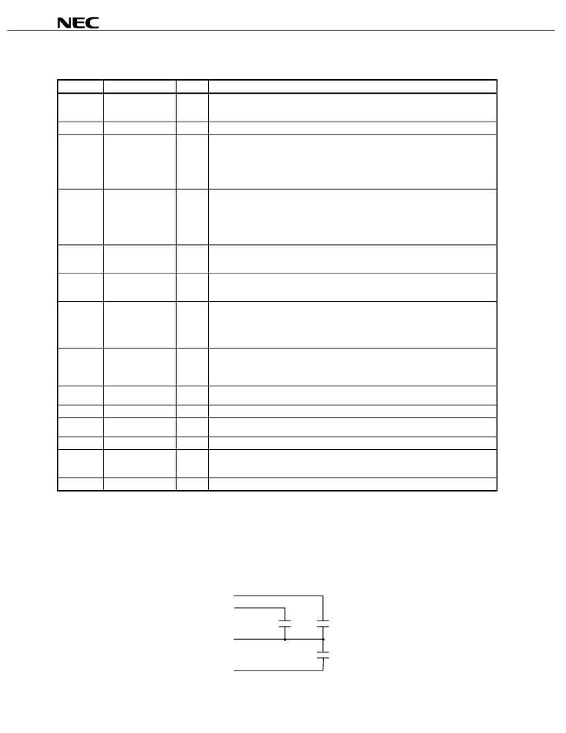
2. Insert a capacitor of about 0.1
μ
F between each power line, as shown below, to secure noise
margin such as V
IH
and V
IL
.
→
logic input
→
V
EE
→
V
DD2
in this order. Turn off power
V
DD2
V
DD1
V
SS
0.1 F
0.1 F
0.1 F
V
EE
相關PDF資料 |
PDF描述 |
|---|---|
| PD54003 | RF POWER TRANSISTORS The LdmoST Plastic FAMILY |
| PD54003-PD54003S | RF POWER TRANSISTORS The LdmoST Plastic FAMILY |
| PD54003S | RF POWER TRANSISTORS The LdmoST Plastic FAMILY |
| PD54008 | RF POWER TRANSISTORS The LdmoST Plastic FAMILY |
| PD54008-PD54008S | RF POWER TRANSISTORS The LdmoST Plastic FAMILY |
相關代理商/技術參數(shù) |
參數(shù)描述 |
|---|---|
| PD16-73 | 制造商:ALPHA 制造商全稱:ALPHA 功能描述:Two-Way 0∑ Power Splitter Combiner 1.42-1.66 GHz |
| PD16-73LF | 制造商:Skyworks Solutions Inc 功能描述:N-WAY DIVIDER / COMBINER |
| PD16-73LF-B | 制造商:Skyworks Solutions Inc 功能描述:N-WAY DIVIDER / COMBINER |
| PD-16A040 | 制造商:VISHAY 制造商全稱:Vishay Siliconix 功能描述:Plasma Panel Displays 16 Character, 16 Segment Alphanumeric Display with .400 [10.16mm] High Characters |
| PD-16A050-3 | 制造商:Vishay Dale 功能描述:- Bulk |
發(fā)布緊急采購,3分鐘左右您將得到回復。