- 您現(xiàn)在的位置:買賣IC網(wǎng) > PDF目錄296796 > PCM9211PTR (TEXAS INSTRUMENTS INC) DATACOM, TOKEN RING TRANSCEIVER, PQFP48 PDF資料下載
參數(shù)資料
| 型號(hào): | PCM9211PTR |
| 廠商: | TEXAS INSTRUMENTS INC |
| 元件分類: | 網(wǎng)絡(luò)接口 |
| 英文描述: | DATACOM, TOKEN RING TRANSCEIVER, PQFP48 |
| 封裝: | GREEN, PLASTIC, LQFP-48 |
| 文件頁(yè)數(shù): | 59/121頁(yè) |
| 文件大?。?/td> | 1219K |
| 代理商: | PCM9211PTR |
第1頁(yè)第2頁(yè)第3頁(yè)第4頁(yè)第5頁(yè)第6頁(yè)第7頁(yè)第8頁(yè)第9頁(yè)第10頁(yè)第11頁(yè)第12頁(yè)第13頁(yè)第14頁(yè)第15頁(yè)第16頁(yè)第17頁(yè)第18頁(yè)第19頁(yè)第20頁(yè)第21頁(yè)第22頁(yè)第23頁(yè)第24頁(yè)第25頁(yè)第26頁(yè)第27頁(yè)第28頁(yè)第29頁(yè)第30頁(yè)第31頁(yè)第32頁(yè)第33頁(yè)第34頁(yè)第35頁(yè)第36頁(yè)第37頁(yè)第38頁(yè)第39頁(yè)第40頁(yè)第41頁(yè)第42頁(yè)第43頁(yè)第44頁(yè)第45頁(yè)第46頁(yè)第47頁(yè)第48頁(yè)第49頁(yè)第50頁(yè)第51頁(yè)第52頁(yè)第53頁(yè)第54頁(yè)第55頁(yè)第56頁(yè)第57頁(yè)第58頁(yè)當(dāng)前第59頁(yè)第60頁(yè)第61頁(yè)第62頁(yè)第63頁(yè)第64頁(yè)第65頁(yè)第66頁(yè)第67頁(yè)第68頁(yè)第69頁(yè)第70頁(yè)第71頁(yè)第72頁(yè)第73頁(yè)第74頁(yè)第75頁(yè)第76頁(yè)第77頁(yè)第78頁(yè)第79頁(yè)第80頁(yè)第81頁(yè)第82頁(yè)第83頁(yè)第84頁(yè)第85頁(yè)第86頁(yè)第87頁(yè)第88頁(yè)第89頁(yè)第90頁(yè)第91頁(yè)第92頁(yè)第93頁(yè)第94頁(yè)第95頁(yè)第96頁(yè)第97頁(yè)第98頁(yè)第99頁(yè)第100頁(yè)第101頁(yè)第102頁(yè)第103頁(yè)第104頁(yè)第105頁(yè)第106頁(yè)第107頁(yè)第108頁(yè)第109頁(yè)第110頁(yè)第111頁(yè)第112頁(yè)第113頁(yè)第114頁(yè)第115頁(yè)第116頁(yè)第117頁(yè)第118頁(yè)第119頁(yè)第120頁(yè)第121頁(yè)
SBAS495 – JUNE 2010
www.ti.com
MPIO Description
Overview
The PCM9211 offers significant flexibility through its MPIO pins. Depending on the system partitioning of the
specific end product, the pins can be reconfigured to offer various I/Os that complement the design.
There are 14 flexible pins: 12 are Input/Output pins, and two pins that are output only.
The 12 multi-purpose I/O (MPIO) pins are grouped into three banks, each with four pins: MPIO_A, MPIO_B, and
MPIO_C.
The two multi-purpose outputs (MPO) pins are assigned as MPO0 and MPO1.
Assignable Signals for MPIO Pins
The PCM9211 has the following signals that can be brought out to MPIOs. Not all MPIOs are equal; be sure to
review subsequent sections in this document to see which signals can be brought out to which MPIO. The
possible signals are summarized in Table 11.
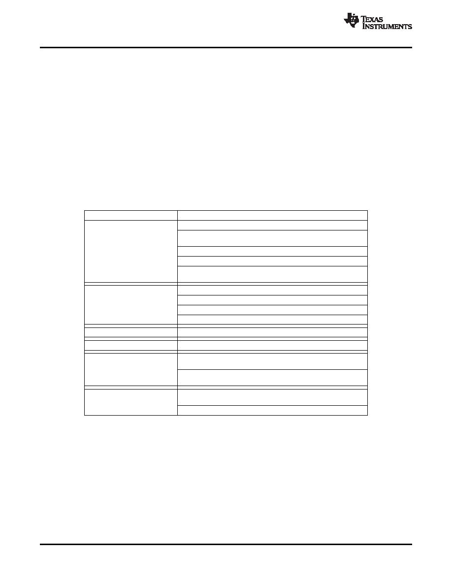
Table 11. Allowable MPIO Signals
MODULE
ALLOWABLE SIGNALS
Extended biphase input pins for DIR: RXIN8/RXIN9/RXIN10/RXIN11
DIR Flags Output: The details of each signal are described in the Flag
section.
DIR
DIR Interrupt Output: INT0 and INT1
DIR, B frame, serial output of channel status, user data, validity flag
DIR, decoded result of sampling frequency calculated by built-in fS
counter
AUXIN0, external serial audio data input (SCK/BCK/LRCK/Data)
AUXIN1, external serial audio data input (SCK/BCK/LRCK/Data)
Auxiliary I/O
AUXIN2, external serial audio data input (SCK/BCK/LRCK/Data)
AUXOUT, external serial audio data output (SCK/BCK/LRCK/Data)
ADC
Serial audio data output for ADC Standalone Operation
DIT
Serial audio data input for DIT Standalone Operation
AVR Application1: Clock Transition Output, Validity Output, XTI
buffered Output, Interrupt Output
Application-Specific
AVR Application2: Secondary BCK/LRCK Output, XTI buffered
Output, Interrupt Output
GPIO (General Purpose I/O), Logical high or low I/O, selectable I/O
Digital Logic Specific
direction for each pin
Hi-Z status, selectable for each pin
How to Assign Functions to MPIO
Both MPO0 and MPO1 have a function assignment register. The output of MPO0 can be selected using the
MPO0SEL[3:0] register; in the same way, the output of MPO1 can be selected using the MPO1SEL[3:0] register.
Selecting the biphase source can be done using Register 35h/RO0SEL and Register 36h/RO1SEL. Muting the
MPO can be done using Registers MPO0MUT and MPO1MUT.
Selection Of Output Source
The PCM9211 also has a routing function for serial digital audio clocks and data. This function routes between all
input sources (DIR, ADC, AUXIN0, AUXIN1, AUXIN2) and Main Out, AUXOUT, and DIT. The selection for Main
Out and AUXOUT is set with these registers:
Main Out: Registers 6Bh, MOSSRC[2:0], and MOPSRC[2:0]
AUXOUT: Register 6Ch, AOSSRC[2:0], and AOPSC[2:0]
42
Copyright 2010, Texas Instruments Incorporated
Product Folder Link(s): PCM9211
相關(guān)PDF資料 |
PDF描述 |
|---|---|
| PCM9211PT | DATACOM, TOKEN RING TRANSCEIVER, PQFP48 |
| PCN11MF | STRIP TERMINAL BLOCK, 1 DECK |
| PCN12E-32S-2.54DSA | 32 CONTACT(S), FEMALE, STRAIGHT TWO PART EURO CONNECTOR, SOLDER, SOCKET |
| PCN12E-44S-2.54DSA | 44 CONTACT(S), FEMALE, STRAIGHT TWO PART EURO CONNECTOR, SOLDER, SOCKET |
| PCN12E-50S-2.54DSA | 50 CONTACT(S), FEMALE, STRAIGHT TWO PART EURO CONNECTOR, SOLDER, SOCKET |
相關(guān)代理商/技術(shù)參數(shù) |
參數(shù)描述 |
|---|---|
| PCM-93 | 功能描述:電線鑒定 Pre-Printed WM Card, Vinyl Cloth, .22" W RoHS:否 制造商:TE Connectivity / Q-Cees 產(chǎn)品:Labels and Signs 類型: 材料:Vinyl 顏色:Blue 寬度:0.625 in 長(zhǎng)度:1 in |
| PCM-9342 | 制造商:ADVANTECH 制造商全稱:Advantech Co., Ltd. 功能描述:X86 SoC 3.5" SBC with VGA, LCD, LAN, USB, SATA, CF, PC/104 |
| PCM-9342F-64A1E | 制造商:ADVANTECH 制造商全稱:Advantech Co., Ltd. 功能描述:X86 SoC 3.5" SBC with VGA, LCD, LAN, USB, SATA, CF, PC/104 |
| PCM-9342FZ2-64A1E | 制造商:ADVANTECH 制造商全稱:Advantech Co., Ltd. 功能描述:X86 SoC 3.5" SBC with VGA, LCD, LAN, USB, SATA, CF, PC/104 |
| PCM-9342L-64A1E | 制造商:ADVANTECH 制造商全稱:Advantech Co., Ltd. 功能描述:X86 SoC 3.5" SBC with VGA, LCD, LAN, USB, SATA, CF, PC/104 |
發(fā)布緊急采購(gòu),3分鐘左右您將得到回復(fù)。