- 您現(xiàn)在的位置:買(mǎi)賣(mài)IC網(wǎng) > PDF目錄382382 > PCF8576U (NXP SEMICONDUCTORS) Universal LCD driver for low multiplex rates PDF資料下載
參數(shù)資料
| 型號(hào): | PCF8576U |
| 廠商: | NXP SEMICONDUCTORS |
| 元件分類: | 顯示驅(qū)動(dòng)器 |
| 英文描述: | Universal LCD driver for low multiplex rates |
| 中文描述: | LIQUID CRYSTAL DISPLAY DRIVER, UUC56 |
| 封裝: | DIE |
| 文件頁(yè)數(shù): | 8/40頁(yè) |
| 文件大小: | 243K |
| 代理商: | PCF8576U |
第1頁(yè)第2頁(yè)第3頁(yè)第4頁(yè)第5頁(yè)第6頁(yè)第7頁(yè)當(dāng)前第8頁(yè)第9頁(yè)第10頁(yè)第11頁(yè)第12頁(yè)第13頁(yè)第14頁(yè)第15頁(yè)第16頁(yè)第17頁(yè)第18頁(yè)第19頁(yè)第20頁(yè)第21頁(yè)第22頁(yè)第23頁(yè)第24頁(yè)第25頁(yè)第26頁(yè)第27頁(yè)第28頁(yè)第29頁(yè)第30頁(yè)第31頁(yè)第32頁(yè)第33頁(yè)第34頁(yè)第35頁(yè)第36頁(yè)第37頁(yè)第38頁(yè)第39頁(yè)第40頁(yè)

1998 Feb 06
8
Philips Semiconductors
Product specification
Universal LCD driver for low multiplex
rates
PCF8576
6.1
Power-on reset
At power-on the PCF8576 resets to a starting condition as
follows:
1.
All backplane outputs are set to V
DD
.
2.
All segment outputs are set to V
DD
.
3.
The drive mode ‘1 : 4 multiplex with
1
3
bias’ is selected.
4.
Blinking is switched off.
5.
Input and output bank selectors are reset (as defined
in Table 5).
6.
The I
2
C-bus interface is initialized.
7.
The data pointer and the subaddress counter are
cleared.
Data transfers on the I
2
C-bus should be avoided for 1 ms
following power-on to allow completion of the reset action.
6.2
LCD bias generator
The full-scale LCD voltage (V
op
) is obtained from
V
DD
V
LCD
. The LCD voltage may be temperature
compensated externally through the V
LCD
supply to pin 12.
Fractional LCD biasing voltages are obtained from an
internal voltage divider of the three series resistors
connected between V
DD
and V
LCD
. The centre resistor can
be switched out of the circuit to provide a
1
2
bias voltage
level for the 1 : 2 multiplex configuration.
6.3
LCD voltage selector
The LCD voltage selector co-ordinates the multiplexing of
the LCD in accordance with the selected LCD drive
configuration. The operation of the voltage selector is
controlled by MODE SET commands from the command
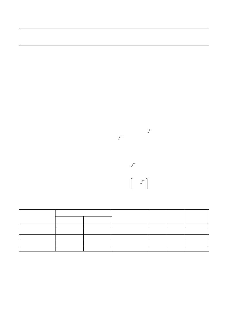
decoder. The biasing configurations that apply to the
preferred modes of operation, together with the biasing
characteristics as functions of V
op
= V
DD
V
LCD
and the
resulting discrimination ratios (D), are given in Table 2.
A practical value for V
op
is determined by equating V
off(rms)
with a defined LCD threshold voltage (V
th
), typically when
the LCD exhibits approximately 10% contrast. In the static
drive mode a suitable choice is V
op
> 3V
th
approximately.
Multiplex drive ratios of 1 : 3 and 1 : 4 with
1
2
bias are
possible but the discrimination and hence the contrast
ratios are smaller (
= 1.732 for 1 : 3 multiplex or
= 1.528 for 1 : 4 multiplex).
The advantage of these modes is a reduction of the LCD
full-scale voltage V
op
as follows:
1 : 3 multiplex (
1
2
bias):
×
V
op
=
= 2.449 V
off(rms)
1 : 4 multiplex (
1
2
bias):
V
op
=
= 2.309 V
off(rms)
These compare with V
op
= 3 V
off(rms)
when
1
3
bias is used.
3
3
----21
6
V
off rms
3
×
)
3
--4
Table 2
Preferred LCD drive modes: summary of characteristics
LCD DRIVE MODE
NUMBER OF
LCD BIAS
CONFIGURATION
BACKPLANES
LEVELS
static
1 : 2
1 : 2
1 : 3
1 : 4
1
2
2
3
4
2
3
4
4
4
static
1
2
1
3
1
3
1
3
0
1
∞
0.354
0.333
0.333
0.333
0.791
0.745
0.638
0.577
2.236
2.236
1.915
1.732
V
op
----V
V
op
----V
D
V
off(rms)
V
=
相關(guān)PDF資料 |
PDF描述 |
|---|---|
| PCF8577C | LCD direct/duplex driver with I2C-bus interface |
| PCF8577CP | LCD direct/duplex driver with I2C-bus interface |
| PCF8591 | 8-bit A/D and D/A converter |
| PCA8591 | 8-bit A/D and D/A converter |
| PCA8591P | 8-bit A/D and D/A converter |
相關(guān)代理商/技術(shù)參數(shù) |
參數(shù)描述 |
|---|---|
| PCF8576U/10 | 制造商:PHILIPS 制造商全稱:NXP Semiconductors 功能描述:Universal LCD driver for low multiplex rates |
| PCF8576U/12 | 制造商:PHILIPS 制造商全稱:NXP Semiconductors 功能描述:Universal LCD driver for low multiplex rates |
| PCF8576U/2 | 制造商:PHILIPS 制造商全稱:NXP Semiconductors 功能描述:Universal LCD driver for low multiplex rates |
| PCF8576U/5 | 制造商:PHILIPS 制造商全稱:NXP Semiconductors 功能描述:Universal LCD driver for low multiplex rates |
| PCF8576U/7 | 制造商:PHILIPS 制造商全稱:NXP Semiconductors 功能描述:Universal LCD driver for low multiplex rates |
發(fā)布緊急采購(gòu),3分鐘左右您將得到回復(fù)。