- 您現(xiàn)在的位置:買賣IC網(wǎng) > PDF目錄382381 > PCF5079HK (NXP Semiconductors N.V.) 3455RMG Series Phenolic Manual Reset Thermostats PDF資料下載
參數(shù)資料
| 型號(hào): | PCF5079HK |
| 廠商: | NXP Semiconductors N.V. |
| 英文描述: | 3455RMG Series Phenolic Manual Reset Thermostats |
| 中文描述: | 3455RMG 系列酚醛手動(dòng)重置恒溫器 |
| 文件頁數(shù): | 25/28頁 |
| 文件大?。?/td> | 146K |
| 代理商: | PCF5079HK |
第1頁第2頁第3頁第4頁第5頁第6頁第7頁第8頁第9頁第10頁第11頁第12頁第13頁第14頁第15頁第16頁第17頁第18頁第19頁第20頁第21頁第22頁第23頁第24頁當(dāng)前第25頁第26頁第27頁第28頁

2001 Nov 21
25
Philips Semiconductors
Product specification
Dual-band power amplifier controller for
GSM, PCN and DCS
PCF5079
15 SOLDERING (HVSON10)
15.1
Soldering information
Informationcontainedwithinthischapterisofapreliminary
nature and may change without notice.
15.2
PCB design guidelines
These guidelines are to help the user in developing the
properPCBdesign. Forthesurface mountprocessreferto
“Data Handbook IC26; Integrated Circuit Packages”
(document order number 9398 652 90011).
15.2.1
P
ERIMETER PAD DESIGN
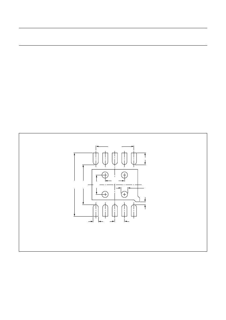
Referring to Fig.20, dimensions Z and G are respectively
the outside to outside and the inside to inside pad
dimensions.
The dimensions X and Y indicate respectively the width
and the length of the pad. Note that the calculated
X dimension is the maximum value in order to avoid solder
bridging between adjacent pads.The calculated
Y dimension is the minimum value and therefore pad
design should start with this value and the pad length at
the outside be extended if more solder joint fillets are
required.
The dimension ‘Cpl’ defines the minimum distance
between the inner tip of the pad and the outer edge of the
thermal pad. It is suggested that this dimension be fixed at
0.15 mm to avoid solder bridging issues between the
thermal pad and the perimeter pads.
handbook, full pagewidth
MGW498
Cpl = 0.15
0.33
Z = 3.27
Y = 0.55
G =
2.09
1.20
1.00
X = 0.28
0.50
TYP
2.00 REF
1.20
1.00
Fig.20 HVSON10 PCB pattern.
Dimensions in mm.
The solder mask opening dimension should be larger than the pad dimension by 125 to 150
μ
m.
15.2.2
T
HERMAL PAD AND VIA DESIGN
The size of the thermal pad should at least match the size
of the exposed die-attach paddle. However, in some
cases, the die-attach paddle size may need to be modified
to avoid solder bridging between the thermal pad and the
perimeter pads. In order to effectively transfer heat from
the top metal layer to the inner or bottom layers of the
PCB, thermal vias should be incorporated into the thermal
pad design. The number of thermal vias will depend on the
application and on the power dissipation and electrical
requirements. It is recommended to incorporate an array
of thermal vias at a pitch of 1.0 to 1.2 mm with the via
diameter between 0.3 and 0.33 mm.
相關(guān)PDF資料 |
PDF描述 |
|---|---|
| PCF5079T | Dual-band power amplifier controller for GSM, PCN and DCS |
| PCF5081 | STEEL COVER |
| PCF5082 | GSM baseband processors for digital mobile cellular radio |
| PCF5083 | STEEL COVER |
| PCF84C12A | 8-BIT MICROCONTROLLER |
相關(guān)代理商/技術(shù)參數(shù) |
參數(shù)描述 |
|---|---|
| PCF5079T | 制造商:PHILIPS 制造商全稱:NXP Semiconductors 功能描述:Dual-band power amplifier controller for GSM, PCN and DCS |
| PCF5081 | 制造商:PHILIPS 制造商全稱:NXP Semiconductors 功能描述:GSM baseband processors for digital mobile cellular radio |
| PCF5082 | 制造商:PHILIPS 制造商全稱:NXP Semiconductors 功能描述:GSM baseband processors for digital mobile cellular radio |
| PCF5083 | 制造商:PHILIPS 制造商全稱:NXP Semiconductors 功能描述:GSM signal processing IC |
| PCF5083H/001/F2 | 制造商:PHILIPS 制造商全稱:NXP Semiconductors 功能描述:GSM signal processing IC |
發(fā)布緊急采購,3分鐘左右您將得到回復(fù)。