- 您現(xiàn)在的位置:買賣IC網(wǎng) > PDF目錄12010 > P89V52X2FBD,157 (NXP Semiconductors)IC 80C51 MCU FLASH 8K 44-LQFP PDF資料下載
參數(shù)資料
| 型號: | P89V52X2FBD,157 |
| 廠商: | NXP Semiconductors |
| 文件頁數(shù): | 9/57頁 |
| 文件大?。?/td> | 0K |
| 描述: | IC 80C51 MCU FLASH 8K 44-LQFP |
| 產(chǎn)品培訓模塊: | Migrating from 8/16-Bit MCUs to 32-Bit ARMs |
| 標準包裝: | 800 |
| 系列: | 89V |
| 核心處理器: | 8051 |
| 芯體尺寸: | 8-位 |
| 速度: | 40MHz |
| 連通性: | UART/USART |
| 外圍設備: | POR |
| 輸入/輸出數(shù): | 32 |
| 程序存儲器容量: | 8KB(8K x 8) |
| 程序存儲器類型: | 閃存 |
| EEPROM 大小: | 192 x 8 |
| RAM 容量: | 256 x 8 |
| 電壓 - 電源 (Vcc/Vdd): | 2.7 V ~ 5.5 V |
| 振蕩器型: | 外部 |
| 工作溫度: | -40°C ~ 85°C |
| 封裝/外殼: | 44-LQFP |
| 包裝: | 托盤 |
| 配用: | 622-1017-ND - BOARD 44-ZIF PLCC SOCKET 622-1012-ND - BOARD FOR P89V52X2 44-TQFP 622-1008-ND - BOARD FOR LPC9103 10-HVSON |
| 其它名稱: | 568-4250 935282529157 P89V52X2FBD |
第1頁第2頁第3頁第4頁第5頁第6頁第7頁第8頁當前第9頁第10頁第11頁第12頁第13頁第14頁第15頁第16頁第17頁第18頁第19頁第20頁第21頁第22頁第23頁第24頁第25頁第26頁第27頁第28頁第29頁第30頁第31頁第32頁第33頁第34頁第35頁第36頁第37頁第38頁第39頁第40頁第41頁第42頁第43頁第44頁第45頁第46頁第47頁第48頁第49頁第50頁第51頁第52頁第53頁第54頁第55頁第56頁第57頁
P89V52X2_3
NXP B.V. 2009. All rights reserved.
Product data sheet
Rev. 03 — 4 May 2009
17 of 57
NXP Semiconductors
P89V52X2
80C51 with 256 B RAM, 192 B data EEPROM
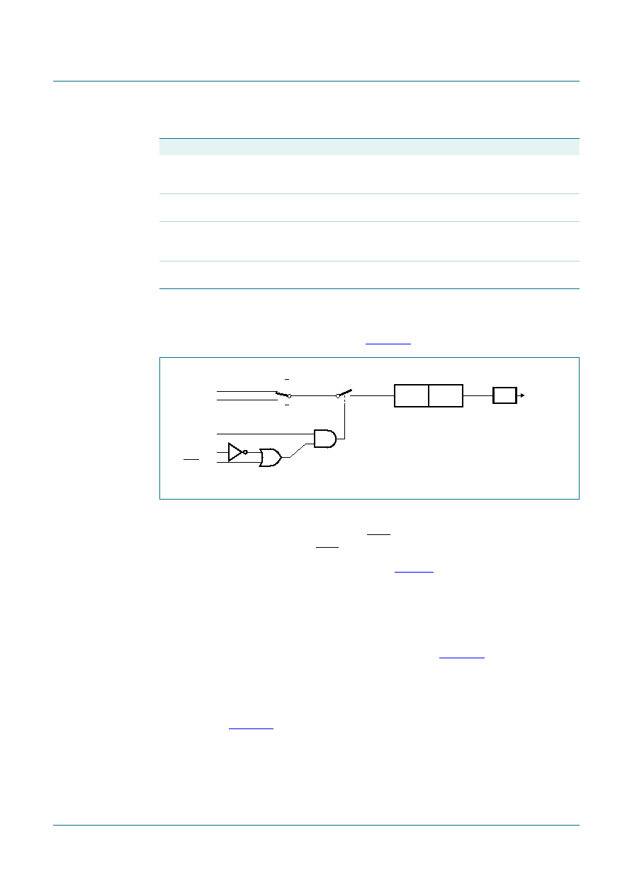
6.8.1 Mode 0
Putting either Timer into Mode 0 makes it look like an 8048 Timer, which is an 8-bit
Counter with a xed divide-by-32 prescaler. Figure 10 shows Mode 0 operation.
In this mode, the Timer register is congured as a 13-bit register. As the count rolls over
from all 1s to all 0s, it sets the Timer interrupt ag TFn. The count input is enabled to the
Timer when TRn = 1 and either GATE = 0 or INTn = 1. (Setting GATE = 1 allows the Timer
to be controlled by external input INTn, to facilitate pulse width measurements). TRn is a
control bit in the Special Function Register TCON (Figure 8). The GATE bit is in the TMOD
register.
The 13-bit register consists of all 8 bits of THn and the lower 5 bits of TLn. The upper
3 bits of TLn are indeterminate and should be ignored. Setting the run ag (TRn) does not
clear the registers.
Mode 0 operation is the same for Timer 0 and Timer 1 (see Figure 10). There are two
different GATE bits, one for Timer 1 (TMOD.7) and one for Timer 0 (TMOD.3).
6.8.2 Mode 1
Mode 1 is the same as Mode 0, except that all 16 bits of the timer register (THn and TLn)
are used. See Figure 11.
3
IE1
Interrupt 1 Edge ag. Set by hardware when external interrupt 1
edge/LOW-level is detected. Cleared by hardware when the interrupt
is processed, or by software.
2
IT1
Interrupt 1 Type control bit. Set/cleared by software to specify falling
edge/LOW-level that triggers external interrupt 1.
1
IE0
Interrupt 0 Edge ag. Set by hardware when external interrupt 0
edge/LOW-level is detected. Cleared by hardware when the interrupt
is processed, or by software.
0
IT0
Interrupt 0 Type control bit. Set/cleared by software to specify falling
edge/LOW-level that triggers external interrupt 0.
Table 14.
TCON - Timer/Counter control register (address 88H) bit description …continued
Bit
Symbol
Description
Fig 10. Timer/Counter 0 or 1 in Mode 0 (13-bit counter)
002aaa519
osc/6
Tn pin
TRn
TnGate
INTn pin
C/T = 0
C/T = 1
TLn
(5-bits)
THn
(8-bits)
TFn
control
overflow
interrupt
相關PDF資料 |
PDF描述 |
|---|---|
| P89V52X2FA,512 | IC 80C51 MCU FLASH 8K 44-PLCC |
| VJ2225Y104KBLAT4X | CAP CER 0.1UF 630V 10% X7R 2225 |
| LPC2292FET144/G,55 | IC ARM7 MCU FLASH 256K 144TFBGA |
| VI-JWM-IY-F4 | CONVERTER MOD DC/DC 10V 50W |
| VI-JWL-IY-F3 | CONVERTER MOD DC/DC 28V 50W |
相關代理商/技術參數(shù) |
參數(shù)描述 |
|---|---|
| P89V52X2FN | 制造商:PHILIPS 制造商全稱:NXP Semiconductors 功能描述:8-bit 80C51 low power 8 kB flash microcontroller with 256 B RAM, 192 B data EEPROM |
| P89V52X2FN,112 | 功能描述:8位微控制器 -MCU 80C51 8K FL / 256 RM RoHS:否 制造商:Silicon Labs 核心:8051 處理器系列:C8051F39x 數(shù)據(jù)總線寬度:8 bit 最大時鐘頻率:50 MHz 程序存儲器大小:16 KB 數(shù)據(jù) RAM 大小:1 KB 片上 ADC:Yes 工作電源電壓:1.8 V to 3.6 V 工作溫度范圍:- 40 C to + 105 C 封裝 / 箱體:QFN-20 安裝風格:SMD/SMT |
| P89V660 | 制造商:PHILIPS 制造商全稱:NXP Semiconductors 功能描述:8-bit 80C51 5 V low power 16 kB/32 kB/64 kB flash microcontroller with 512 B/1 kB/2 kB RAM, dual I2C-bus, SPI |
| P89V660_08 | 制造商:PHILIPS 制造商全稱:NXP Semiconductors 功能描述:8-bit 80C51 5 V low power 16 kB/32 kB/64 kB flash microcontroller with 512 B/1 kB/2 kB RAM, dual I2C-bus, SPI |
| P89V660_0811 | 制造商:PHILIPS 制造商全稱:NXP Semiconductors 功能描述:8-bit 80C51 5 V low power 16 kB/32 kB/64 kB flash microcontroller with 512 B/1 kB/2 kB RAM, dual I2C-bus, SPI |
發(fā)布緊急采購,3分鐘左右您將得到回復。