- 您現(xiàn)在的位置:買賣IC網(wǎng) > PDF目錄384806 > OXFW911 (Electronic Theatre Controls, Inc.) IEEE1394 to ATA/ATAPI Native Bridge PDF資料下載
參數(shù)資料
| 型號: | OXFW911 |
| 廠商: | Electronic Theatre Controls, Inc. |
| 英文描述: | IEEE1394 to ATA/ATAPI Native Bridge |
| 中文描述: | IEEE1394連接到ATA / ATAPI的母語橋 |
| 文件頁數(shù): | 5/32頁 |
| 文件大小: | 141K |
| 代理商: | OXFW911 |
第1頁第2頁第3頁第4頁當前第5頁第6頁第7頁第8頁第9頁第10頁第11頁第12頁第13頁第14頁第15頁第16頁第17頁第18頁第19頁第20頁第21頁第22頁第23頁第24頁第25頁第26頁第27頁第28頁第29頁第30頁第31頁第32頁
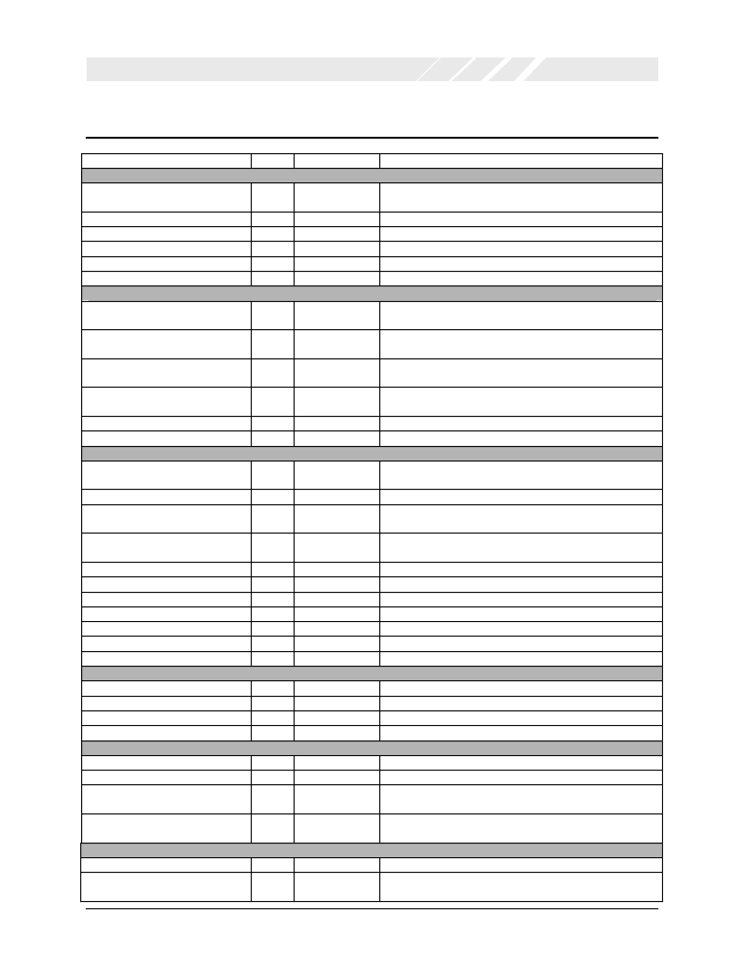
3 P
IN
D
ESCRIPTIONS
Data Sheet Rev 1.1
Page 5
OXFW911
OXFORD SEMICONDUCTOR LTD.
1394 PHY-LINK interface
104, 105, 108, 109, 110, 111, 114,
115
116,117
119
121
102
103
ARM external interface
2, 3, 4, 5, 6, 9, 10, 11, 12, 13, 16,
17, 18, 19, 20, 24
35, 36, 37, 38, 41, 42, 43, 44, 45,
46, 49, 50, 51, 52, 53, 54, 60
123, 124, 27, 33
Dir
1
Name
Description
I/O
PD[7:0]
Phy-Link Data Bus
I/O
I
O
IU
O
CTL[1:0]
PHYCLK
LREQ
LINKON
LPS
Phy-Link Control Bus
49.152 MHz clock sourced by PHY
Link Request
Requests link to power up when in a low power mode
Indicates to phy that link is powered and ready
T_I/O
D[15:0]
ARMexternal data bus
T_O
A[16:0]
ARMexternal address bus
T_O
CS#[3:0]
ARMexternal chip selects. CS0#is always used for program
ROM.
ARMexternal output enable. Active when reading data from
external devices including programROM
Write Enable. Active when writing to external devices
External ARMinterrupt
28
T_O
OE#
34
61
T_O
T_IU
WE#
INT#
IDE interface
86, 82, 80, 78, 74, 72, 70, 66, 65,
69, 71, 73, 77, 79, 81, 85
99, 97, 98
101, 100
T_I/O
ID[15:0]
IDE data bus
T_O
T_O
IA[2:0]
ICS#[1:0]
IDE address bus
IDE chip select. Used to select the Command Block or
Control Block registers.
IDE output enable. Only used when external buffering is
required to drive IDE data bus
IDE interface reset
IDE interface write strobe
IDE interface read strobe
63
T_O
IDE_OE#
64
89
90
91
92
95
62
T_O
T_I
T_O
T_O
T_O
T_O
T_I
IRESET
DMARQ
DIOW#
DIOR#
IORDY
DMACK#
INTRQ
EEPROMinterface
125
126
127
58
O
O
O
GPO1
GPO2
GPO3
GPI
General Purpose Output 1
General Purpose Output 2
General Purpose Output 3
General Purpose Input
T_IU
Miscellaneous Pins
56
128
IU
T_O
I
RESET#
CKOUT
TEST_SEL,
TEST[1:0]
UIF
Global reset for the OXFW911. Active Low.
Clock output. 49.152 MHz clock output.
‘100’ = NORMAL OPERATION. Other settings are for
foundry test purposes only.
Leave unconnected to use internal Flash, tie low to use only
external device
22, 32, 31
57
IU
Power and ground
2
15, 8, 40, 48, 59, 76, 94, 107, 113
30, 21, 23, 68, 84, 88, 120
VDD
VDD
AC VDD
DC VDD
Supplies power to output buffers in switching (AC) state
Power supply. Supplies power to core logic, input buffers
and output buffers in steady state
相關(guān)PDF資料 |
PDF描述 |
|---|---|
| OXFW911-TQ-A | IEEE1394 to ATA/ATAPI Native Bridge |
| OZ6812 | ACPI CardBus Controller |
| OZ6812B | ACPI CardBus Controller |
| OZ6812T | ACPI CardBus Controller |
| OZ6833 | ACPI CardBus Controller |
相關(guān)代理商/技術(shù)參數(shù) |
參數(shù)描述 |
|---|---|
| OXFW911PLUS | 制造商:OXFORD 制造商全稱:OXFORD 功能描述:1394A-to-ATA7/ATAPI Bridge |
| OXFW911-TQ-A | 制造商:未知廠家 制造商全稱:未知廠家 功能描述:IEEE1394 to ATA/ATAPI Native Bridge |
| OXFW912 | 制造商:OXFORD 制造商全稱:OXFORD 功能描述:1394B-to-ATA7/ATAPI Bridge |
| OXFW970-TQAG | 功能描述:USB 接口集成電路 2 in 8 out FireWire audio Cont. RoHS:否 制造商:Cypress Semiconductor 產(chǎn)品:USB 2.0 數(shù)據(jù)速率: 接口類型:SPI 工作電源電壓:3.15 V to 3.45 V 工作電源電流: 最大工作溫度:+ 85 C 安裝風格:SMD/SMT 封裝 / 箱體:WLCSP-20 |
| OXFW971 | 制造商:OXFORD 制造商全稱:OXFORD 功能描述:16 Channel Streaming Audio Firewire I/O Controller with Midi and S/PDIF |
發(fā)布緊急采購,3分鐘左右您將得到回復。