- 您現(xiàn)在的位置:買賣IC網(wǎng) > PDF目錄384806 > OXFW900-TQ-A (Electronic Theatre Controls, Inc.) IEEE1394 to ATA/ATAPI Native Bridge PDF資料下載
參數(shù)資料
| 型號: | OXFW900-TQ-A |
| 廠商: | Electronic Theatre Controls, Inc. |
| 英文描述: | IEEE1394 to ATA/ATAPI Native Bridge |
| 中文描述: | IEEE1394連接到ATA / ATAPI的母語橋 |
| 文件頁數(shù): | 5/30頁 |
| 文件大小: | 187K |
| 代理商: | OXFW900-TQ-A |
第1頁第2頁第3頁第4頁當前第5頁第6頁第7頁第8頁第9頁第10頁第11頁第12頁第13頁第14頁第15頁第16頁第17頁第18頁第19頁第20頁第21頁第22頁第23頁第24頁第25頁第26頁第27頁第28頁第29頁第30頁
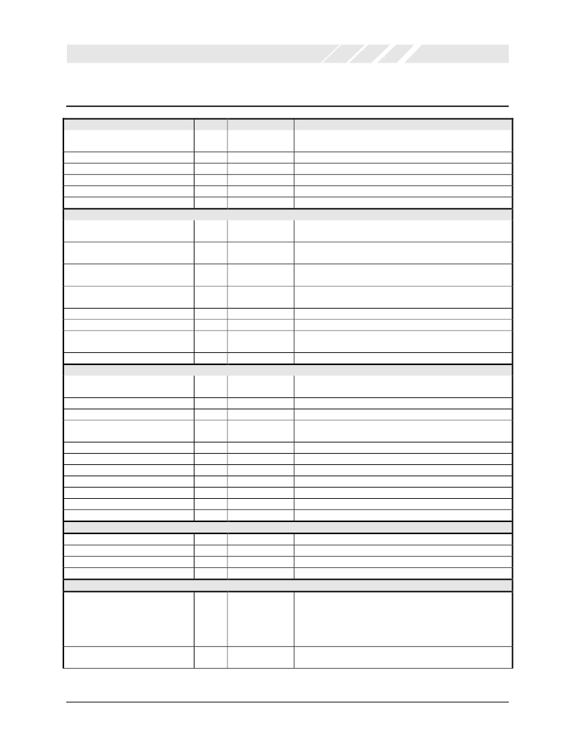
3 P
IN
D
ESCRIPTIONS
Data Sheet Revision 1.0
Page 5
OXFW900
OXFORD SEMICONDUCTOR LTD.
1394 PHY-LINK interface
104, 105, 108, 109, 110, 111, 115,
116
117,118
120
122
102
103
ARMexternal interface
2, 3, 4, 5, 6, 7, 10, 11, 12, 13, 14,
15, 18, 19, 20, 21
35, 36, 37, 40, 41, 42, 43, 44, 45,
48, 49, 50, 51, 52, 53, 54, 60
25, 26, 29, 30
Dir
1
I/O
Name
PD[7:0]
Description
Phy-Link Data Bus
I/O
I
O
IU
O
CTL[1:0]
PHYCLK
LREQ
LINKON
LPS
Phy-Link Control Bus
49.152 MHz clock sourced by PHY
Link Request
Requests link to power up when in a low power mode
Indicates to phy that link is powered and ready
T_I/O
D[15:0]
ARMexternal data bus
T_O
A[16:0]
ARMexternal address bus
T_O
CS#[3:0]
ARMexternal chip selects. CS0#is always used for program
ROM.
ARMexternal output enable. Active when reading data from
external devices including programROM
Byte Write enables. For future expansion
Write Enable. Active when writing to external devices
‘1’ = 16 bit external ROM ‘0’ = 8 bit external ROM
(pulldown)
External ARMinterrupt
31
T_O
OE#
32, 33
34
62
T_O
T_O
ID
BWR#[1:0]
WE#
WIDTH16
61
T_IU
INT#
IDE interface
65, 66, 69, 70, 71, 72, 73, 74, 77,
78, 79, 80, 81, 82, 85, 86
97, 98, 99
100, 101
63
T_I/O
ID[15:0]
IDE data bus
T_O
T_O
T_O
IA[2:0]
ICS#[1:0]
IDE_OE#[
IDE address bus
IDE chip select. Selects IDE drive 0 or 1
IDE output enable. Only used when external buffering is
required to drive IDE data bus
IDE interface reset
IDE interface write strobe
IDE interface read strobe
64
89
90
91
92
95
96
T_O
T_I
T_O
T_O
T_O
T_O
T_I
IRESET
DMARQ
DIOW#
DIOR#
IORDY
DMACK#
INTRQ
EEPROMinterface
128
126
1
127
O
O
IU
O
GPO3
GPO1
GPI
GPO2
General Purpose Output 3
General Purpose Output 1
General Purpose Input
General Purpose Output 2
Mscellaneous Pins
57
I
XTLI
Crystal Oscillator input. 24.576 MHz crystal required. If a
clock module is used rather than a crystal then this input
must be tied high for the OXFW900 to operate, and the clock
module output connected to the CKIN pin. IMPORTANT -
See Application Notes regarding clocking
Crystal Oscillator output. IMPORTANT – See Application
Notes regarding clocking.
58
O
XTLO
相關PDF資料 |
PDF描述 |
|---|---|
| OXFW911 | IEEE1394 to ATA/ATAPI Native Bridge |
| OXFW911-TQ-A | IEEE1394 to ATA/ATAPI Native Bridge |
| OZ6812 | ACPI CardBus Controller |
| OZ6812B | ACPI CardBus Controller |
| OZ6812T | ACPI CardBus Controller |
相關代理商/技術參數(shù) |
參數(shù)描述 |
|---|---|
| OXFW911 | 制造商:未知廠家 制造商全稱:未知廠家 功能描述:IEEE1394 to ATA/ATAPI Native Bridge |
| OXFW911PLUS | 制造商:OXFORD 制造商全稱:OXFORD 功能描述:1394A-to-ATA7/ATAPI Bridge |
| OXFW911-TQ-A | 制造商:未知廠家 制造商全稱:未知廠家 功能描述:IEEE1394 to ATA/ATAPI Native Bridge |
| OXFW912 | 制造商:OXFORD 制造商全稱:OXFORD 功能描述:1394B-to-ATA7/ATAPI Bridge |
| OXFW970-TQAG | 功能描述:USB 接口集成電路 2 in 8 out FireWire audio Cont. RoHS:否 制造商:Cypress Semiconductor 產(chǎn)品:USB 2.0 數(shù)據(jù)速率: 接口類型:SPI 工作電源電壓:3.15 V to 3.45 V 工作電源電流: 最大工作溫度:+ 85 C 安裝風格:SMD/SMT 封裝 / 箱體:WLCSP-20 |
發(fā)布緊急采購,3分鐘左右您將得到回復。