- 您現(xiàn)在的位置:買賣IC網(wǎng) > PDF目錄11731 > ORSO42G5-1BM484I (Lattice Semiconductor Corporation)IC FPSC TRANSCEIVER 4CH 484-BGA PDF資料下載
參數(shù)資料
| 型號(hào): | ORSO42G5-1BM484I |
| 廠商: | Lattice Semiconductor Corporation |
| 文件頁數(shù): | 111/153頁 |
| 文件大小: | 0K |
| 描述: | IC FPSC TRANSCEIVER 4CH 484-BGA |
| 產(chǎn)品變化通告: | Product Discontinuation 01/Aug/2011 |
| 標(biāo)準(zhǔn)包裝: | 60 |
| 系列: | * |
第1頁第2頁第3頁第4頁第5頁第6頁第7頁第8頁第9頁第10頁第11頁第12頁第13頁第14頁第15頁第16頁第17頁第18頁第19頁第20頁第21頁第22頁第23頁第24頁第25頁第26頁第27頁第28頁第29頁第30頁第31頁第32頁第33頁第34頁第35頁第36頁第37頁第38頁第39頁第40頁第41頁第42頁第43頁第44頁第45頁第46頁第47頁第48頁第49頁第50頁第51頁第52頁第53頁第54頁第55頁第56頁第57頁第58頁第59頁第60頁第61頁第62頁第63頁第64頁第65頁第66頁第67頁第68頁第69頁第70頁第71頁第72頁第73頁第74頁第75頁第76頁第77頁第78頁第79頁第80頁第81頁第82頁第83頁第84頁第85頁第86頁第87頁第88頁第89頁第90頁第91頁第92頁第93頁第94頁第95頁第96頁第97頁第98頁第99頁第100頁第101頁第102頁第103頁第104頁第105頁第106頁第107頁第108頁第109頁第110頁當(dāng)前第111頁第112頁第113頁第114頁第115頁第116頁第117頁第118頁第119頁第120頁第121頁第122頁第123頁第124頁第125頁第126頁第127頁第128頁第129頁第130頁第131頁第132頁第133頁第134頁第135頁第136頁第137頁第138頁第139頁第140頁第141頁第142頁第143頁第144頁第145頁第146頁第147頁第148頁第149頁第150頁第151頁第152頁第153頁
Lattice Semiconductor
ORCA ORSO42G5 and ORSO82G5 Data Sheet
60
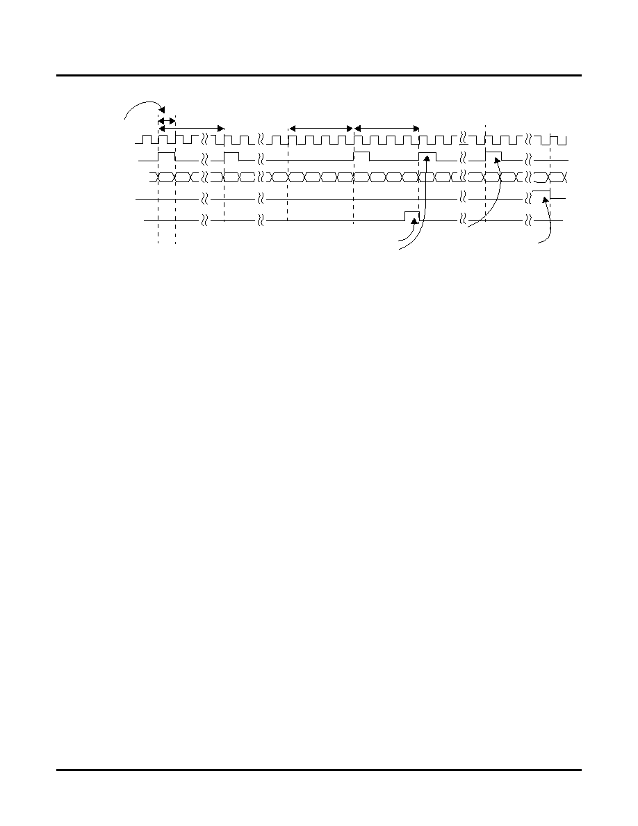
Figure 46. ORSO82G5 Receive FPGA/Embedded Core Interface IPC8 Mode
In the SERDES-only mode the data are simply transferred as 32-bit wide words to and from the FPGA logic. The
next sections describe the signal denitions for the TX and RX paths in the SONET, OPC2 and OPC8 modes. The
signal names unique to an operating mode are preferred for design and are generally the ones used in the
ispLEVER design environment. The labels in the left most column are the hardware FPGA interface names. The
ispLEVER software creates an HDL module with specic names based on the mode selected for each channel.
The interface signals for the embedded RAM are completely independent of these signals. The memory signals are
described in a later section.
Signal Description for TX Path (FPGA to SERDES Core) – ORSO42G5
Signals are divided across four channels with 40 signals per channel. TXDxx[39:0] is the set of 40 signals for a
channel xx.
The data signals multiplexing scheme is similar to the one used for the RXD signals. However, the status signals
multiplexing is different. Please refer to Table 11 for a detailed description of the TXD multiplexing scheme.
For all channels the TXDxx[39:33] signals are not used.
Table 11 summarizes the signals at the FPGA/Core interface in the transmit direction.
SYSCLK156x[1,2]
IPC8_CELLSTART
D
DDD
D
DD
D
DDDD
“n” clk cycles
4 clk cycles
CELL BIP ERROR
If a Cell BIP Error occurs, the CELL_BIP_ERR signal
reects the occurrence, as shown in the figure.
D
IPC8_CELL_BIP_ERR
IPC8_CELLDROP
IPC8_[159:0]
BIP Error is associated
with CURRENT cell
Cell Drop is associated with
the NEXT cell (NOT present)
CELL BIP ERROR
If a cell error occurs within the ASB and;
1. CELL_BIP_INH=0 (Do not drop BIP errored cells)
2. A BIP error occurs
The drop indicator will PRECEED the user cell that con-
tains the BIP error. All data will be passed w/o modica-
tion.
1 cycle
IDLE
相關(guān)PDF資料 |
PDF描述 |
|---|---|
| PIC18F4682-I/ML | IC PIC MCU FLASH 40KX16 44QFN |
| ORT8850L-2BMN680I | IC TRANCEIVERS FPSC 680FPGAM |
| ORT8850L-1BMN680C | IC TRANCEIVERS FPSC 680FPGAM |
| VE-B0B-IX-F1 | CONVERTER MOD DC/DC 95V 75W |
| SY100E446JC TR | IC CONV 4-BIT SER/PAR 28-PLCC |
相關(guān)代理商/技術(shù)參數(shù) |
參數(shù)描述 |
|---|---|
| ORSO42G5-1BMN484C | 功能描述:FPGA - 現(xiàn)場(chǎng)可編程門陣列 10368 LUT 204 I/O RoHS:否 制造商:Altera Corporation 系列:Cyclone V E 柵極數(shù)量: 邏輯塊數(shù)量:943 內(nèi)嵌式塊RAM - EBR:1956 kbit 輸入/輸出端數(shù)量:128 最大工作頻率:800 MHz 工作電源電壓:1.1 V 最大工作溫度:+ 70 C 安裝風(fēng)格:SMD/SMT 封裝 / 箱體:FBGA-256 |
| ORSO42G5-1BMN484I | 功能描述:FPGA - 現(xiàn)場(chǎng)可編程門陣列 10368 LUT 204 I/O RoHS:否 制造商:Altera Corporation 系列:Cyclone V E 柵極數(shù)量: 邏輯塊數(shù)量:943 內(nèi)嵌式塊RAM - EBR:1956 kbit 輸入/輸出端數(shù)量:128 最大工作頻率:800 MHz 工作電源電壓:1.1 V 最大工作溫度:+ 70 C 安裝風(fēng)格:SMD/SMT 封裝 / 箱體:FBGA-256 |
| ORSO42G5-2BM484C | 功能描述:FPGA - 現(xiàn)場(chǎng)可編程門陣列 10368 LUT 204 I/O RoHS:否 制造商:Altera Corporation 系列:Cyclone V E 柵極數(shù)量: 邏輯塊數(shù)量:943 內(nèi)嵌式塊RAM - EBR:1956 kbit 輸入/輸出端數(shù)量:128 最大工作頻率:800 MHz 工作電源電壓:1.1 V 最大工作溫度:+ 70 C 安裝風(fēng)格:SMD/SMT 封裝 / 箱體:FBGA-256 |
| ORSO42G5-2BM484I | 功能描述:FPGA - 現(xiàn)場(chǎng)可編程門陣列 10368 LUT 204 I/O RoHS:否 制造商:Altera Corporation 系列:Cyclone V E 柵極數(shù)量: 邏輯塊數(shù)量:943 內(nèi)嵌式塊RAM - EBR:1956 kbit 輸入/輸出端數(shù)量:128 最大工作頻率:800 MHz 工作電源電壓:1.1 V 最大工作溫度:+ 70 C 安裝風(fēng)格:SMD/SMT 封裝 / 箱體:FBGA-256 |
| ORSO42G5-2BMN484C | 功能描述:FPGA - 現(xiàn)場(chǎng)可編程門陣列 10368 LUT 204 I/O RoHS:否 制造商:Altera Corporation 系列:Cyclone V E 柵極數(shù)量: 邏輯塊數(shù)量:943 內(nèi)嵌式塊RAM - EBR:1956 kbit 輸入/輸出端數(shù)量:128 最大工作頻率:800 MHz 工作電源電壓:1.1 V 最大工作溫度:+ 70 C 安裝風(fēng)格:SMD/SMT 封裝 / 箱體:FBGA-256 |
發(fā)布緊急采購(gòu),3分鐘左右您將得到回復(fù)。