- 您現在的位置:買賣IC網 > PDF目錄299581 > ORLI10G-1BMN416I (LATTICE SEMICONDUCTOR CORP) FPGA, 1296 CLBS, 380000 GATES, PBGA416 PDF資料下載
參數資料
| 型號: | ORLI10G-1BMN416I |
| 廠商: | LATTICE SEMICONDUCTOR CORP |
| 元件分類: | FPGA |
| 英文描述: | FPGA, 1296 CLBS, 380000 GATES, PBGA416 |
| 封裝: | PLASTIC, MULTILAYER, BGA-416 |
| 文件頁數: | 29/74頁 |
| 文件大小: | 1411K |
| 代理商: | ORLI10G-1BMN416I |
第1頁第2頁第3頁第4頁第5頁第6頁第7頁第8頁第9頁第10頁第11頁第12頁第13頁第14頁第15頁第16頁第17頁第18頁第19頁第20頁第21頁第22頁第23頁第24頁第25頁第26頁第27頁第28頁當前第29頁第30頁第31頁第32頁第33頁第34頁第35頁第36頁第37頁第38頁第39頁第40頁第41頁第42頁第43頁第44頁第45頁第46頁第47頁第48頁第49頁第50頁第51頁第52頁第53頁第54頁第55頁第56頁第57頁第58頁第59頁第60頁第61頁第62頁第63頁第64頁第65頁第66頁第67頁第68頁第69頁第70頁第71頁第72頁第73頁第74頁
Agere Systems Inc.
35
Preliminary Data Sheet
March 2001
10 Gbits/s Transmit and Receive Line Interface
ORCA ORLI10G FPSC
XGMII ORCA 4E Receive Analysis (continued)
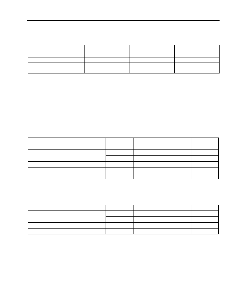
Table 3. Assumed Inputs to FPGA
Absolute Maximum Ratings
Stresses in excess of the absolute maximum ratings can cause permanent damage to the device. These are abso-
lute stress ratings only. Functional operation of the device is not implied at these or any other conditions in excess
of those given in the operations sections of this data sheet. Exposure to absolute maximum ratings for extended
periods can adversely affect device reliability.
The ORCA Series 4 FPSCs include circuitry designed to protect the chips from damaging substrate injection cur-
rents and to prevent accumulations of static charge. Nevertheless, conventional precautions should be observed
during storage, handling, and use to avoid exposure to excessive electrical stress.
Table 4. Absolute Maximum Ratings
Recommended Operating Conditions
Table 5. Recommended Operating Conditions
Inputs
Low
Nom
High
VDDIO
1.4 V
1.5 V
1.6 V
VIH (min level)
0.88 V
0.95 V
1.10 V
VREF
0.68 V
0.75 V
0.90 V
VIL (max level)
0.48 V
0.55 V
0.70 V
Parameter
Symbol
Min
Max
Unit
Storage Temperature
Tstg
–65
150
°C
Power Supply Voltage with Respect to
Ground
VDD3
—
≤4.2
V
VDD15
—
2V
Input Signal with Respect to Ground
—
VSS – 0.3
VDDIO + 0.3
V
Signal Applied to High-impedance Output
—
VSS – 0.3
VDDIO + 0.3
V
Maximum Package Body Temperature
——
220
°C
Parameter
Symbol
Min
Max
Unit
Power Supply Voltage with Respect to
Ground
VDD32.7
3.6
V
VDD15
1.4
1.6
V
Input Voltages
VIN
VSS – 0.3
VDDIO + 0.3
V
Junction Temperature
TJ
–40
125
°C
相關PDF資料 |
PDF描述 |
|---|---|
| ORLI10G-1BM416 | FPGA, 1296 CLBS, 380000 GATES, PBGA416 |
| ORLI10G-1BM680 | FPGA, 1296 CLBS, 380000 GATES, PBGA680 |
| ORLI10G-2BM416 | FPGA, 1296 CLBS, 380000 GATES, PBGA416 |
| ORLI10G-2BM680 | FPGA, 1296 CLBS, 380000 GATES, PBGA680 |
| ORLI10G-3BM416 | FPGA, 1296 CLBS, 380000 GATES, PBGA416 |
相關代理商/技術參數 |
參數描述 |
|---|---|
| ORLI10G-1BMN680C | 功能描述:FPGA - 現場可編程門陣列 10368 LUT 316 I/O RoHS:否 制造商:Altera Corporation 系列:Cyclone V E 柵極數量: 邏輯塊數量:943 內嵌式塊RAM - EBR:1956 kbit 輸入/輸出端數量:128 最大工作頻率:800 MHz 工作電源電壓:1.1 V 最大工作溫度:+ 70 C 安裝風格:SMD/SMT 封裝 / 箱體:FBGA-256 |
| ORLI10G-1BMN680I | 功能描述:FPGA - 現場可編程門陣列 10368 LUT 316 I/O RoHS:否 制造商:Altera Corporation 系列:Cyclone V E 柵極數量: 邏輯塊數量:943 內嵌式塊RAM - EBR:1956 kbit 輸入/輸出端數量:128 最大工作頻率:800 MHz 工作電源電壓:1.1 V 最大工作溫度:+ 70 C 安裝風格:SMD/SMT 封裝 / 箱體:FBGA-256 |
| ORLI10G-2BM680C | 功能描述:FPGA - 現場可編程門陣列 10368 LUT 316 I/O RoHS:否 制造商:Altera Corporation 系列:Cyclone V E 柵極數量: 邏輯塊數量:943 內嵌式塊RAM - EBR:1956 kbit 輸入/輸出端數量:128 最大工作頻率:800 MHz 工作電源電壓:1.1 V 最大工作溫度:+ 70 C 安裝風格:SMD/SMT 封裝 / 箱體:FBGA-256 |
| ORLI10G-2BM680I | 功能描述:FPGA - 現場可編程門陣列 10368 LUT 316 I/O RoHS:否 制造商:Altera Corporation 系列:Cyclone V E 柵極數量: 邏輯塊數量:943 內嵌式塊RAM - EBR:1956 kbit 輸入/輸出端數量:128 最大工作頻率:800 MHz 工作電源電壓:1.1 V 最大工作溫度:+ 70 C 安裝風格:SMD/SMT 封裝 / 箱體:FBGA-256 |
| ORLI10G-2BMN680C | 功能描述:FPGA - 現場可編程門陣列 10368 LUT 316 I/O RoHS:否 制造商:Altera Corporation 系列:Cyclone V E 柵極數量: 邏輯塊數量:943 內嵌式塊RAM - EBR:1956 kbit 輸入/輸出端數量:128 最大工作頻率:800 MHz 工作電源電壓:1.1 V 最大工作溫度:+ 70 C 安裝風格:SMD/SMT 封裝 / 箱體:FBGA-256 |
發(fā)布緊急采購,3分鐘左右您將得到回復。