- 您現(xiàn)在的位置:買賣IC網(wǎng) > PDF目錄299576 > OR3T80-4BC432I FPGA, 484 CLBS, 58000 GATES, 80 MHz, PBGA432 PDF資料下載
參數(shù)資料
| 型號(hào): | OR3T80-4BC432I |
| 元件分類: | FPGA |
| 英文描述: | FPGA, 484 CLBS, 58000 GATES, 80 MHz, PBGA432 |
| 封裝: | BGA-432 |
| 文件頁(yè)數(shù): | 155/210頁(yè) |
| 文件大小: | 2138K |
| 代理商: | OR3T80-4BC432I |
第1頁(yè)第2頁(yè)第3頁(yè)第4頁(yè)第5頁(yè)第6頁(yè)第7頁(yè)第8頁(yè)第9頁(yè)第10頁(yè)第11頁(yè)第12頁(yè)第13頁(yè)第14頁(yè)第15頁(yè)第16頁(yè)第17頁(yè)第18頁(yè)第19頁(yè)第20頁(yè)第21頁(yè)第22頁(yè)第23頁(yè)第24頁(yè)第25頁(yè)第26頁(yè)第27頁(yè)第28頁(yè)第29頁(yè)第30頁(yè)第31頁(yè)第32頁(yè)第33頁(yè)第34頁(yè)第35頁(yè)第36頁(yè)第37頁(yè)第38頁(yè)第39頁(yè)第40頁(yè)第41頁(yè)第42頁(yè)第43頁(yè)第44頁(yè)第45頁(yè)第46頁(yè)第47頁(yè)第48頁(yè)第49頁(yè)第50頁(yè)第51頁(yè)第52頁(yè)第53頁(yè)第54頁(yè)第55頁(yè)第56頁(yè)第57頁(yè)第58頁(yè)第59頁(yè)第60頁(yè)第61頁(yè)第62頁(yè)第63頁(yè)第64頁(yè)第65頁(yè)第66頁(yè)第67頁(yè)第68頁(yè)第69頁(yè)第70頁(yè)第71頁(yè)第72頁(yè)第73頁(yè)第74頁(yè)第75頁(yè)第76頁(yè)第77頁(yè)第78頁(yè)第79頁(yè)第80頁(yè)第81頁(yè)第82頁(yè)第83頁(yè)第84頁(yè)第85頁(yè)第86頁(yè)第87頁(yè)第88頁(yè)第89頁(yè)第90頁(yè)第91頁(yè)第92頁(yè)第93頁(yè)第94頁(yè)第95頁(yè)第96頁(yè)第97頁(yè)第98頁(yè)第99頁(yè)第100頁(yè)第101頁(yè)第102頁(yè)第103頁(yè)第104頁(yè)第105頁(yè)第106頁(yè)第107頁(yè)第108頁(yè)第109頁(yè)第110頁(yè)第111頁(yè)第112頁(yè)第113頁(yè)第114頁(yè)第115頁(yè)第116頁(yè)第117頁(yè)第118頁(yè)第119頁(yè)第120頁(yè)第121頁(yè)第122頁(yè)第123頁(yè)第124頁(yè)第125頁(yè)第126頁(yè)第127頁(yè)第128頁(yè)第129頁(yè)第130頁(yè)第131頁(yè)第132頁(yè)第133頁(yè)第134頁(yè)第135頁(yè)第136頁(yè)第137頁(yè)第138頁(yè)第139頁(yè)第140頁(yè)第141頁(yè)第142頁(yè)第143頁(yè)第144頁(yè)第145頁(yè)第146頁(yè)第147頁(yè)第148頁(yè)第149頁(yè)第150頁(yè)第151頁(yè)第152頁(yè)第153頁(yè)第154頁(yè)當(dāng)前第155頁(yè)第156頁(yè)第157頁(yè)第158頁(yè)第159頁(yè)第160頁(yè)第161頁(yè)第162頁(yè)第163頁(yè)第164頁(yè)第165頁(yè)第166頁(yè)第167頁(yè)第168頁(yè)第169頁(yè)第170頁(yè)第171頁(yè)第172頁(yè)第173頁(yè)第174頁(yè)第175頁(yè)第176頁(yè)第177頁(yè)第178頁(yè)第179頁(yè)第180頁(yè)第181頁(yè)第182頁(yè)第183頁(yè)第184頁(yè)第185頁(yè)第186頁(yè)第187頁(yè)第188頁(yè)第189頁(yè)第190頁(yè)第191頁(yè)第192頁(yè)第193頁(yè)第194頁(yè)第195頁(yè)第196頁(yè)第197頁(yè)第198頁(yè)第199頁(yè)第200頁(yè)第201頁(yè)第202頁(yè)第203頁(yè)第204頁(yè)第205頁(yè)第206頁(yè)第207頁(yè)第208頁(yè)第209頁(yè)第210頁(yè)
Lucent Technologies Inc.
49
Preliminary Data Sheet, Rev. 1
September 1998
ORCA Series 3 FPGAs
Clock Distribution Network (continued)
Clock Sources to the PLC Array
The source of a clock that is globally available to the
PLC array can be from any user I/O pad, any of the
ExpressCLK
pads, or an internally generated source.
System Clock
As described in the Programmable Input/Output Cells
section, PICs are grouped in adjacent pairs. Any one of
the eight pads in a PIC pair can drive a clock spine in a
row or column. For PIC pairs on the top of the chip, the
column associated with the left PIC has the clock
spine, for pairs on the bottom, the right PIC column has
the spine. The top PIC of the pair sources the spine
from the left side of the array, and the bottom PIC of the
pair sources the spine from the right side of the array.
Clock delay and skew are minimized by having a single
clock buffer per pair of PICs. The clock spine for each
pair can also be driven by one of the four PIC switching
segments (pSW) in each PIC of the pair. This allows a
signal generated in the PLC array to be routed onto the
global clock spine network. The system clock output of
the programmable clock manager (PCM) may also be
routed to the global system clock spines via the pSW
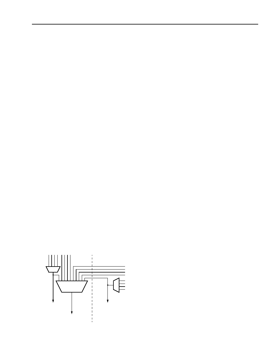
segments. Figure 33 shows the clock spine multiplex-
ing structure for a pair of PICs on the top of the array.
Fast Clock
The Fast Clock spines are sourced to the PLC array
from each side of the device by the ExpressCLK pads
via the CLKCNTRL function block (described in the
Special Function Blocks section). The ExpressCLK and
Fast Clock source from the pads is shown in Figure 34
and will be described further in the ExpressCLK Inputs
subsection.
Figure 33. PIC System Clock Spine Generation
Clocks in the PICs
Because the Series 3 FPGAs have latches and FFs in
the I/Os, it is necessary to have clock signal distribution
to the PIOs as well as in the PLC array. The system
clock, the Fast Clock, and the ExpressCLK are avail-
able for PIO clocking.
PIC System Clock
There are five local system clock lines in each PIC.
Much like the sources for a clock in the PFU, two of the
local PIC clocks are generated within the PIC from long
lines. One is generated from the set of ten PIC long
lines (pxL) that runs parallel to the PICs on a side, and
the other is generated from the set of ten long lines (xL)
from the PLC array that terminate in the PIC. Another
local PIC system clock route comes from the set of ten
xL lines in the adjacent PLC that is parallel to the side
of the array on which the PIC resides. The fourth local
PIC system clock route comes from the set of ten long
lines (xL) from the PLC array that terminate in the adja-
cent PIC that is not part of the same PIC pair. Much like
the E1 signals in the PLCs that are used to distribute a
local clock to the PFU source, the fifth local clock line in
each PIC comes from local PSW signals. This clock
signal for each PIC is shown in Figure 33. One of these
five local PIC system clocks is selected for the system
clock signal in the PIO. It is used as the PIO system
clock for both input and output clocking as selected
within the PIO. All PIOs in a PIC share the same sys-
tem clock.
PIC ExpressCLK
The ExpressCLK signal used at the PIC latches/FFs
comes from the CLKCNTRL function block that resides
in the middle of the side on which the PIC resides. The
ExpressCLK
output from the CLKCNTRL block is
divided into two signals, although the same Express-
CLK
source from the pads or the programmable clock
manager (PCM) feeds both signals. One ExpressCLK
signal goes to the PICs on the right of (above) the
CLKCNTRL block, and the other ExpressCLK signal
goes to the PICs on the left of (below) the CLKCNTRL
block on that side.
PAD A
PAD B
PAD C
PAD D
PSW[4]
PSW[5]
PSW[6]
PSW[7]
PA
D
A
PA
D
B
PA
D
C
PA
D
PS
W
[4
]
PS
W
[5
]
PS
W
[6
]
PS
W
[7
]
TO LOCAL CLOCKS
SPINE
5-5800(F)
相關(guān)PDF資料 |
PDF描述 |
|---|---|
| OR3C80-4BC600I | FPGA, 484 CLBS, 58000 GATES, 80 MHz, PBGA600 |
| OR3C80-5BC600I | FPGA, 484 CLBS, 58000 GATES, 80 MHz, PBGA600 |
| OR3T125-4BC600I | FPGA, 784 CLBS, 92000 GATES, 80 MHz, PBGA600 |
| OR3T80-4BC600I | FPGA, 484 CLBS, 58000 GATES, 80 MHz, PBGA600 |
| OR3T80-5BC600I | FPGA, 484 CLBS, 58000 GATES, 80 MHz, PBGA600 |
相關(guān)代理商/技術(shù)參數(shù) |
參數(shù)描述 |
|---|---|
| OR3T80-4BC600I | 制造商:未知廠家 制造商全稱:未知廠家 功能描述:Field Programmable Gate Array (FPGA) |
| OR3T80-4PS208I | 制造商:未知廠家 制造商全稱:未知廠家 功能描述:Field Programmable Gate Array (FPGA) |
| OR3T80-4PS240I | 制造商:未知廠家 制造商全稱:未知廠家 功能描述:Field Programmable Gate Array (FPGA) |
| OR3T80-5BA352 | 制造商:AGERE 制造商全稱:AGERE 功能描述:3C and 3T Field-Programmable Gate Arrays |
| OR3T80-5BA352I | 制造商:AGERE 制造商全稱:AGERE 功能描述:3C and 3T Field-Programmable Gate Arrays |
發(fā)布緊急采購(gòu),3分鐘左右您將得到回復(fù)。