- 您現(xiàn)在的位置:買賣IC網(wǎng) > PDF目錄299576 > OR3T165-4PS240 FPGA, 1024 CLBS, 120000 GATES, PQFP240 PDF資料下載
參數(shù)資料
| 型號: | OR3T165-4PS240 |
| 元件分類: | FPGA |
| 英文描述: | FPGA, 1024 CLBS, 120000 GATES, PQFP240 |
| 封裝: | SQFP-240 |
| 文件頁數(shù): | 175/210頁 |
| 文件大?。?/td> | 2138K |
| 代理商: | OR3T165-4PS240 |
第1頁第2頁第3頁第4頁第5頁第6頁第7頁第8頁第9頁第10頁第11頁第12頁第13頁第14頁第15頁第16頁第17頁第18頁第19頁第20頁第21頁第22頁第23頁第24頁第25頁第26頁第27頁第28頁第29頁第30頁第31頁第32頁第33頁第34頁第35頁第36頁第37頁第38頁第39頁第40頁第41頁第42頁第43頁第44頁第45頁第46頁第47頁第48頁第49頁第50頁第51頁第52頁第53頁第54頁第55頁第56頁第57頁第58頁第59頁第60頁第61頁第62頁第63頁第64頁第65頁第66頁第67頁第68頁第69頁第70頁第71頁第72頁第73頁第74頁第75頁第76頁第77頁第78頁第79頁第80頁第81頁第82頁第83頁第84頁第85頁第86頁第87頁第88頁第89頁第90頁第91頁第92頁第93頁第94頁第95頁第96頁第97頁第98頁第99頁第100頁第101頁第102頁第103頁第104頁第105頁第106頁第107頁第108頁第109頁第110頁第111頁第112頁第113頁第114頁第115頁第116頁第117頁第118頁第119頁第120頁第121頁第122頁第123頁第124頁第125頁第126頁第127頁第128頁第129頁第130頁第131頁第132頁第133頁第134頁第135頁第136頁第137頁第138頁第139頁第140頁第141頁第142頁第143頁第144頁第145頁第146頁第147頁第148頁第149頁第150頁第151頁第152頁第153頁第154頁第155頁第156頁第157頁第158頁第159頁第160頁第161頁第162頁第163頁第164頁第165頁第166頁第167頁第168頁第169頁第170頁第171頁第172頁第173頁第174頁當前第175頁第176頁第177頁第178頁第179頁第180頁第181頁第182頁第183頁第184頁第185頁第186頁第187頁第188頁第189頁第190頁第191頁第192頁第193頁第194頁第195頁第196頁第197頁第198頁第199頁第200頁第201頁第202頁第203頁第204頁第205頁第206頁第207頁第208頁第209頁第210頁
Preliminary Data Sheet, Rev. 1
September 1998
ORCA Series 3 FPGAs
Lucent Technologies Inc.
67
Microprocessor Interface (MPI) (continued)
Status Register
The microprocessor interface status register is a read-only register, providing information to the host processor.
Configuration Data Register
The MPI configuration data register is a writable register in configuration mode and a readable register in readback
mode. For FPGA configuration, this is where the configuration data bytes are sequentially written by the host pro-
cessor. Similarly, for readback mode, the MPI provides the readback data bytes in this register for the host proces-
sor.
Readback Address Register 1
The MPI readback address register 1 is a writable register used to accept the least significant address byte
(bits [7:0]) of the configuration data location to be read back.
Readback Address Register 2
The MPI readback address register 2 is a writable register used to accept the most significant address byte
(bits [15:8]) of the configuration data location to be read back.
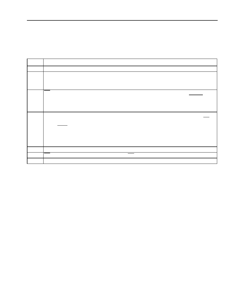
Table 22. Status Register
Bit #
Description
Bit 0
Reserved.
Bit 1
Data Ready. Set by the MPI, a 1 on this bit during configuration alerts the host processor that the FPGA
is ready for another byte of configuration data. During byte-wide readback, the MPI sets this bit to a 1 to
tell the host processor that a byte of configuration data is available for reading. This bit is cleared by a
host processor access (read or write) to the configuration data register.
Bit 2
IRQ
Pending. The MPI sets this bit to 1 to indicate to the host processor that the FPGA has a pending
interrupt request. This bit may be used for the host processor to poll for interrupts if the MPI_IRQ pin out-
put of the FPGA has been masked at the host processor. This bit is set to 0 when the status register is
read. Interrupt requests from the FPGA user space must be cleared in FPGA user logic in addition to
reading this bit.
Bits [4:3] Bit Stream Error Flags. Bits 3 and 4 are set by the MPI to indicate any error during FPGA configura-
tion. See bit 2 of control register 2 for the capability to alert the host processor of an error via the IRQ sig-
nal during configuration. In the truth table below, bit 3 is the LSB (bit on right). These bits are cleared to
0 when PRGM goes active:
00 = No error
01 = ID error
10 = Checksum error
11 = Stop-bit/alignment error
Bit 5
Reserved.
Bit 6
INIT.
This bit reflects the binary value of the FPGA INIT pin.
Bit 7
DONE. This bit reflects the binary value of the FPGA DONE pin.
相關PDF資料 |
PDF描述 |
|---|---|
| OR3T165-5B432 | FPGA, 1024 CLBS, 120000 GATES, PBGA432 |
| OR3T165-5B600 | FPGA, 1024 CLBS, 120000 GATES, PBGA600 |
| OR3T165-5BA352I | FPGA, 1024 CLBS, 120000 GATES, PBGA352 |
| OR3T165-5BA352 | FPGA, 1024 CLBS, 120000 GATES, PBGA352 |
| OR3T165-5BC432I | FPGA, 1024 CLBS, 120000 GATES, PBGA432 |
相關代理商/技術參數(shù) |
參數(shù)描述 |
|---|---|
| OR3T20 | 制造商:AGERE 制造商全稱:AGERE 功能描述:3C and 3T Field-Programmable Gate Arrays |
| OR3T20-4BA256I | 制造商:未知廠家 制造商全稱:未知廠家 功能描述:Field Programmable Gate Array (FPGA) |
| OR3T20-4S208I | 制造商:未知廠家 制造商全稱:未知廠家 功能描述:Field Programmable Gate Array (FPGA) |
| OR3T20-4S240I | 制造商:未知廠家 制造商全稱:未知廠家 功能描述:Field Programmable Gate Array (FPGA) |
| OR3T20-5BA256 | 制造商:AGERE 制造商全稱:AGERE 功能描述:3C and 3T Field-Programmable Gate Arrays |
發(fā)布緊急采購,3分鐘左右您將得到回復。