- 您現(xiàn)在的位置:買賣IC網(wǎng) > PDF目錄299576 > OR3T165-4PS240 FPGA, 1024 CLBS, 120000 GATES, PQFP240 PDF資料下載
參數(shù)資料
| 型號(hào): | OR3T165-4PS240 |
| 元件分類: | FPGA |
| 英文描述: | FPGA, 1024 CLBS, 120000 GATES, PQFP240 |
| 封裝: | SQFP-240 |
| 文件頁數(shù): | 138/210頁 |
| 文件大小: | 2138K |
| 代理商: | OR3T165-4PS240 |
第1頁第2頁第3頁第4頁第5頁第6頁第7頁第8頁第9頁第10頁第11頁第12頁第13頁第14頁第15頁第16頁第17頁第18頁第19頁第20頁第21頁第22頁第23頁第24頁第25頁第26頁第27頁第28頁第29頁第30頁第31頁第32頁第33頁第34頁第35頁第36頁第37頁第38頁第39頁第40頁第41頁第42頁第43頁第44頁第45頁第46頁第47頁第48頁第49頁第50頁第51頁第52頁第53頁第54頁第55頁第56頁第57頁第58頁第59頁第60頁第61頁第62頁第63頁第64頁第65頁第66頁第67頁第68頁第69頁第70頁第71頁第72頁第73頁第74頁第75頁第76頁第77頁第78頁第79頁第80頁第81頁第82頁第83頁第84頁第85頁第86頁第87頁第88頁第89頁第90頁第91頁第92頁第93頁第94頁第95頁第96頁第97頁第98頁第99頁第100頁第101頁第102頁第103頁第104頁第105頁第106頁第107頁第108頁第109頁第110頁第111頁第112頁第113頁第114頁第115頁第116頁第117頁第118頁第119頁第120頁第121頁第122頁第123頁第124頁第125頁第126頁第127頁第128頁第129頁第130頁第131頁第132頁第133頁第134頁第135頁第136頁第137頁當(dāng)前第138頁第139頁第140頁第141頁第142頁第143頁第144頁第145頁第146頁第147頁第148頁第149頁第150頁第151頁第152頁第153頁第154頁第155頁第156頁第157頁第158頁第159頁第160頁第161頁第162頁第163頁第164頁第165頁第166頁第167頁第168頁第169頁第170頁第171頁第172頁第173頁第174頁第175頁第176頁第177頁第178頁第179頁第180頁第181頁第182頁第183頁第184頁第185頁第186頁第187頁第188頁第189頁第190頁第191頁第192頁第193頁第194頁第195頁第196頁第197頁第198頁第199頁第200頁第201頁第202頁第203頁第204頁第205頁第206頁第207頁第208頁第209頁第210頁
Preliminary Data Sheet, Rev. 1
September 1998
ORCA Series 3 FPGAs
Lucent Technologies Inc.
33
Programmable Input/Output Cells
The programmable input/output cells (PICs) are
located along the perimeter of the device. The PIC’s
name is represented by a two-letter designation to indi-
cate on which side of the device it is located followed
by a number to indicate in which row or column it is
located. The first letter, P, designates that the cell is a
PIC and not a PLC. The second letter indicates the
side of the array where the PIC is located. The four
sides are left (L), right (R), top (T), and bottom (B). The
individual I/O pad is indicated by a single letter (either
A, B, C, or D) placed at the end of the PIC name. As an
example, PL10A indicates a pad located on the left
side of the array in the tenth row.
Each PIC interfaces to four bond pads and contains the
necessary routing resources to provide an interface
between I/O pads and the PLCs. Each PIC is com-
posed of four programmable I/Os (PIOs) and signifi-
cant routing resources. Each PIO contains input
buffers, output buffers, routing resources, latches/FFs,
and logic and can be configured as an input, output, or
bidirectional I/O.
PICs in the Series 3 FPGAs have significant local rout-
ing resources, similar to routing in the PLCs. This new
routing increases the ability to fix user pinouts prior to
placement and routing of a design and still maintain
routability. The flexibility provided by the routing also
provides for increased signal speed due to a greater
variety of signal paths possible.
Included in the PIC routing is a fast path from the input
pins to the SLICs in each of the three adjacent PLCs
(one orthogonal and two diagonal). This feature allows
for input signals to be very quickly processed by the
SLIC decoder function and used on-chip or sent back
off of the FPGA. Also new to the Series 3 PIOs are
latches and FFs and options for using fast, dedicated
clocks called ExpressCLKs. These features will all be
discussed in subsequent sections.
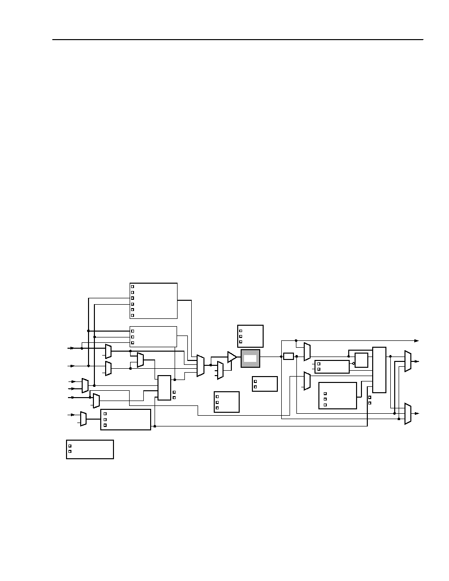
A diagram of a single PIO (one of four in a PIC) is
shown in Figure 22. Table 9 provides an overview of
the programmable functions in an I/O cell.
Key: PD = programmable delay.
Figure 22. OR3C/Txxx Programmable Input/Output (PIO) Image from
ORCA Foundry
5-5805(F)
IN2
IN1
D0
D1
CK
SP
SD
LSR
INREGMODE
LATCHFF
LATCH
FF
D
CK
NORMAL
INVERTED
RESET
SET
LEVEL MODE
TTL
CMOS
UP
DOWN
NONE
PULL-DOWN
BUFFER MODE
TS
FAST
SLEW
SINK
RESET
SET
LSR
SP
CK
D
OUT1
OUT2
ECLK
SCLK
CE
CE_OVER_LSR
LSR_OVER_CE
ASYNC
LSR
ENABLE_GSR
DISABLE_GSR
OUT1OUTREG
OUT2OUTREG
OUT1OUT2
NOR
XOR
XNOR
AND
NAND
OR
PIO LOGIC
CLKIN
0
1
0
PAD
Q
1
PD
Q
1
ECLK
SCLK
PMUX
相關(guān)PDF資料 |
PDF描述 |
|---|---|
| OR3T165-5B432 | FPGA, 1024 CLBS, 120000 GATES, PBGA432 |
| OR3T165-5B600 | FPGA, 1024 CLBS, 120000 GATES, PBGA600 |
| OR3T165-5BA352I | FPGA, 1024 CLBS, 120000 GATES, PBGA352 |
| OR3T165-5BA352 | FPGA, 1024 CLBS, 120000 GATES, PBGA352 |
| OR3T165-5BC432I | FPGA, 1024 CLBS, 120000 GATES, PBGA432 |
相關(guān)代理商/技術(shù)參數(shù) |
參數(shù)描述 |
|---|---|
| OR3T20 | 制造商:AGERE 制造商全稱:AGERE 功能描述:3C and 3T Field-Programmable Gate Arrays |
| OR3T20-4BA256I | 制造商:未知廠家 制造商全稱:未知廠家 功能描述:Field Programmable Gate Array (FPGA) |
| OR3T20-4S208I | 制造商:未知廠家 制造商全稱:未知廠家 功能描述:Field Programmable Gate Array (FPGA) |
| OR3T20-4S240I | 制造商:未知廠家 制造商全稱:未知廠家 功能描述:Field Programmable Gate Array (FPGA) |
| OR3T20-5BA256 | 制造商:AGERE 制造商全稱:AGERE 功能描述:3C and 3T Field-Programmable Gate Arrays |
發(fā)布緊急采購,3分鐘左右您將得到回復(fù)。