- 您現(xiàn)在的位置:買賣IC網 > PDF目錄299576 > OR3T165-4PS208I FPGA, 1024 CLBS, 120000 GATES, PQFP208 PDF資料下載
參數(shù)資料
| 型號: | OR3T165-4PS208I |
| 元件分類: | FPGA |
| 英文描述: | FPGA, 1024 CLBS, 120000 GATES, PQFP208 |
| 封裝: | SQFP-208 |
| 文件頁數(shù): | 79/210頁 |
| 文件大?。?/td> | 2138K |
| 代理商: | OR3T165-4PS208I |
第1頁第2頁第3頁第4頁第5頁第6頁第7頁第8頁第9頁第10頁第11頁第12頁第13頁第14頁第15頁第16頁第17頁第18頁第19頁第20頁第21頁第22頁第23頁第24頁第25頁第26頁第27頁第28頁第29頁第30頁第31頁第32頁第33頁第34頁第35頁第36頁第37頁第38頁第39頁第40頁第41頁第42頁第43頁第44頁第45頁第46頁第47頁第48頁第49頁第50頁第51頁第52頁第53頁第54頁第55頁第56頁第57頁第58頁第59頁第60頁第61頁第62頁第63頁第64頁第65頁第66頁第67頁第68頁第69頁第70頁第71頁第72頁第73頁第74頁第75頁第76頁第77頁第78頁當前第79頁第80頁第81頁第82頁第83頁第84頁第85頁第86頁第87頁第88頁第89頁第90頁第91頁第92頁第93頁第94頁第95頁第96頁第97頁第98頁第99頁第100頁第101頁第102頁第103頁第104頁第105頁第106頁第107頁第108頁第109頁第110頁第111頁第112頁第113頁第114頁第115頁第116頁第117頁第118頁第119頁第120頁第121頁第122頁第123頁第124頁第125頁第126頁第127頁第128頁第129頁第130頁第131頁第132頁第133頁第134頁第135頁第136頁第137頁第138頁第139頁第140頁第141頁第142頁第143頁第144頁第145頁第146頁第147頁第148頁第149頁第150頁第151頁第152頁第153頁第154頁第155頁第156頁第157頁第158頁第159頁第160頁第161頁第162頁第163頁第164頁第165頁第166頁第167頁第168頁第169頁第170頁第171頁第172頁第173頁第174頁第175頁第176頁第177頁第178頁第179頁第180頁第181頁第182頁第183頁第184頁第185頁第186頁第187頁第188頁第189頁第190頁第191頁第192頁第193頁第194頁第195頁第196頁第197頁第198頁第199頁第200頁第201頁第202頁第203頁第204頁第205頁第206頁第207頁第208頁第209頁第210頁
Preliminary Data Sheet, Rev. 1
September 1998
ORCA Series 3 FPGAs
Lucent Technologies Inc.
17
Programmable Logic Cells (continued)
Data is written to the write data, write address, and
write enable registers on the active edge of the clock,
but data is not written into the RAM until the next clock
edge one-half cycle later. The read port is actually
asynchronous, providing the user with read data very
quickly after setting the read address, but timing is also
provided so that the read port may be treated as fully
synchronous for write then read applications. If the
read and write address lines are tied together (main-
taining MSB to MSB, etc.), then the dual-port RAM
operates as a synchronous single-port RAM. If the
write enable is disabled, and an initial memory contents
is provided at configuration time, the memory acts as a
ROM (the write data and write address ports and write
port enables are not used).
Wider memories can be created by operating two or
more memory mode PFUs in parallel, all with the same
address and control signals, but each with a different
nibble of data. To increase memory word depth above
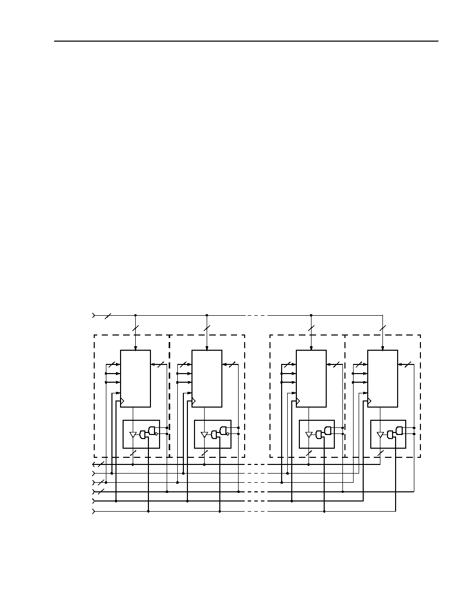
32, two or more PLCs can be used. Figure 10 shows a
128 x 8 dual-port RAM that is implemented in eight
PLCs. This figure demonstrates data path width expan-
sion by placing two memories in parallel to achieve an
8-bit data path. Depth expansion is applied to achieve
128 words deep using the 32-word deep PFU memo-
ries. In addition to the PFU in each PLC, the SLIC
(described in the next section) in each PLC is used for
read address decodes and 3-state drivers. The 128 x 8
RAM shown could be made to operate as a single-port
RAM by tying (bit-for-bit) the read and write addresses.
To achieve depth expansion, one or two of the write
address bits (generally the MSBs) are routed to the
write port enables as in Figure 10. For 2 bits, the bits
select which 32-word bank of RAM of the four available
from a decode of two WPE inputs is to be written. Simi-
larly, 2 bits of the read address are decoded in the
SLIC and are used to control the 3-state buffers
through which the read data passes. The write data
bus is common, with separate nibbles for width expan-
sion, across all PLCs, and the read data bus is com-
mon (again, with separate nibbles) to all PLCs at the
output of the 3-state buffers.
Figure 10 also shows a new optional capability to pro-
vide a read enable for RAMs/ROMs in Series 3 using
the SLIC cell. The read enable will 3-state the read
data bus when inactive, allowing the write data and
read data buses to be tied together if desired.
Figure 10. Memory Mode Expansion Example—128 x 8 RAM
5-5749(F)
RD[7:0]
WE
WA[6:0]
RA[6:0]
CLK
WA
RA
WPE0
WPE1
WE
WD[7:4]
5
4
PLC
8
WD[7:0]
8
7
WA
RA
WPE0
WPE1
WE
RD[3:0]
WD[3:0]
5
4
PLC
RD[7:4]
WA
RA
WPE0
WPE1
WE
WD[7:4]
5
4
PLC
WA
RA
WPE0
WPE1
WE
RD[3:0]
WD[3:0]
5
4
PLC
RD[7:4]
RE
4
PFU
SLIC
相關PDF資料 |
PDF描述 |
|---|---|
| OR3T165-4PS208 | FPGA, 1024 CLBS, 120000 GATES, PQFP208 |
| OR3T165-4PS240I | FPGA, 1024 CLBS, 120000 GATES, PQFP240 |
| OR3T165-4PS240 | FPGA, 1024 CLBS, 120000 GATES, PQFP240 |
| OR3T165-5B432 | FPGA, 1024 CLBS, 120000 GATES, PBGA432 |
| OR3T165-5B600 | FPGA, 1024 CLBS, 120000 GATES, PBGA600 |
相關代理商/技術參數(shù) |
參數(shù)描述 |
|---|---|
| OR3T20 | 制造商:AGERE 制造商全稱:AGERE 功能描述:3C and 3T Field-Programmable Gate Arrays |
| OR3T20-4BA256I | 制造商:未知廠家 制造商全稱:未知廠家 功能描述:Field Programmable Gate Array (FPGA) |
| OR3T20-4S208I | 制造商:未知廠家 制造商全稱:未知廠家 功能描述:Field Programmable Gate Array (FPGA) |
| OR3T20-4S240I | 制造商:未知廠家 制造商全稱:未知廠家 功能描述:Field Programmable Gate Array (FPGA) |
| OR3T20-5BA256 | 制造商:AGERE 制造商全稱:AGERE 功能描述:3C and 3T Field-Programmable Gate Arrays |
發(fā)布緊急采購,3分鐘左右您將得到回復。