- 您現(xiàn)在的位置:買賣IC網(wǎng) > PDF目錄299576 > OR3T165-4PS208I FPGA, 1024 CLBS, 120000 GATES, PQFP208 PDF資料下載
參數(shù)資料
| 型號: | OR3T165-4PS208I |
| 元件分類: | FPGA |
| 英文描述: | FPGA, 1024 CLBS, 120000 GATES, PQFP208 |
| 封裝: | SQFP-208 |
| 文件頁數(shù): | 189/210頁 |
| 文件大?。?/td> | 2138K |
| 代理商: | OR3T165-4PS208I |
第1頁第2頁第3頁第4頁第5頁第6頁第7頁第8頁第9頁第10頁第11頁第12頁第13頁第14頁第15頁第16頁第17頁第18頁第19頁第20頁第21頁第22頁第23頁第24頁第25頁第26頁第27頁第28頁第29頁第30頁第31頁第32頁第33頁第34頁第35頁第36頁第37頁第38頁第39頁第40頁第41頁第42頁第43頁第44頁第45頁第46頁第47頁第48頁第49頁第50頁第51頁第52頁第53頁第54頁第55頁第56頁第57頁第58頁第59頁第60頁第61頁第62頁第63頁第64頁第65頁第66頁第67頁第68頁第69頁第70頁第71頁第72頁第73頁第74頁第75頁第76頁第77頁第78頁第79頁第80頁第81頁第82頁第83頁第84頁第85頁第86頁第87頁第88頁第89頁第90頁第91頁第92頁第93頁第94頁第95頁第96頁第97頁第98頁第99頁第100頁第101頁第102頁第103頁第104頁第105頁第106頁第107頁第108頁第109頁第110頁第111頁第112頁第113頁第114頁第115頁第116頁第117頁第118頁第119頁第120頁第121頁第122頁第123頁第124頁第125頁第126頁第127頁第128頁第129頁第130頁第131頁第132頁第133頁第134頁第135頁第136頁第137頁第138頁第139頁第140頁第141頁第142頁第143頁第144頁第145頁第146頁第147頁第148頁第149頁第150頁第151頁第152頁第153頁第154頁第155頁第156頁第157頁第158頁第159頁第160頁第161頁第162頁第163頁第164頁第165頁第166頁第167頁第168頁第169頁第170頁第171頁第172頁第173頁第174頁第175頁第176頁第177頁第178頁第179頁第180頁第181頁第182頁第183頁第184頁第185頁第186頁第187頁第188頁當(dāng)前第189頁第190頁第191頁第192頁第193頁第194頁第195頁第196頁第197頁第198頁第199頁第200頁第201頁第202頁第203頁第204頁第205頁第206頁第207頁第208頁第209頁第210頁
8
Lucent Technologies Inc.
Preliminary Data Sheet, Rev. 1
ORCA Series 3 FPGAs
September 1998
Programmable Logic Cells
The programmable logic cell (PLC) consists of a pro-
grammable function unit (PFU), a supplemental logic
and interconnect cell (SLIC), and routing resources. All
PLCs in the array are functionally identical with only
minor differences in routing connectivity for improved
routability. The PFU, which contains eight 4-input LUTs,
eight latches/FFs, and one FF for logic implementation,
is discussed in the next section, followed by discus-
sions of the SLIC and PLC routing resources.
Programmable Function Unit
The PFUs are used for logic. Each PFU has 50 exter-
nal inputs and 18 outputs and can operate in several
modes. The functionality of the inputs and outputs
depends on the operating mode.
The PFU uses 36 data input lines for the LUTs, eight
data input lines for the latches/FFs, five control inputs
(ASWE, CLK, CE, LSR, SEL), and a carry input (CIN)
for fast arithmetic functions and general-purpose data
input for the ninth FF. There are eight combinatorial
data outputs (one from each LUT), eight latched/
registered outputs (one from each latch/FF), a carry-
out (COUT), and a registered carry-out (REGCOUT)
that comes from the ninth FF. The carry-out signals are
used principally for fast arithmetic functions.
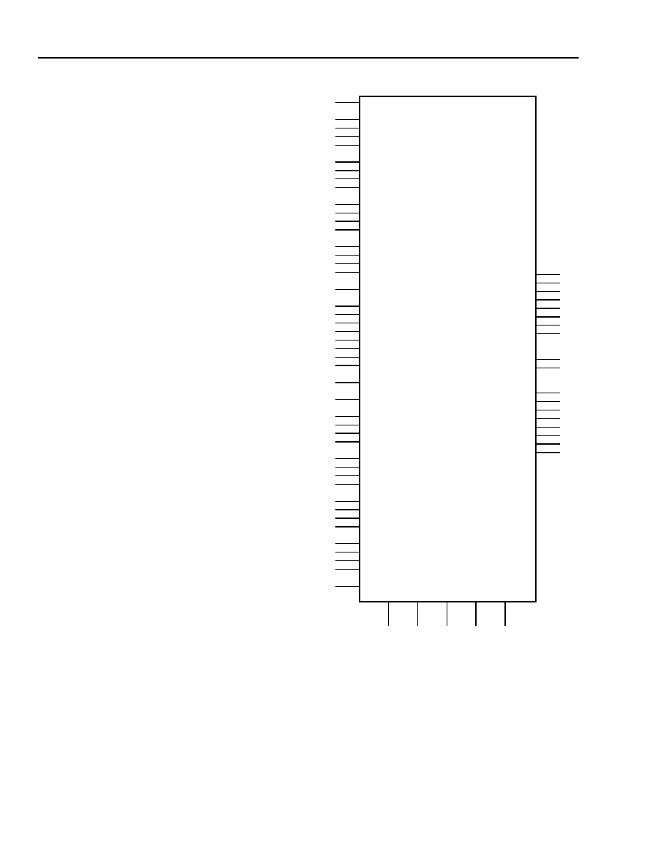
Figure 2 and Figure 3 show high-level and detailed
views of the ports in the PFU, respectively. The eight
sets of LUT inputs are labeled as K0 through K7 with
each of the four inputs to each LUT having a suffix of
_x, where x is a number from 0 to 3. There are four F5
inputs labeled A through D. These inputs are used for a
fifth LUT input for 5-input LUTs or as a selector for mul-
tiplexing two 4-input LUTs. The eight direct data inputs
to the latches/FFs are labeled as DIN[7:0]. Registered
LUT outputs are shown as Q[7:0], and combinatorial
LUT outputs are labeled as F[7:0].
The PFU implements combinatorial logic in the LUTs
and sequential logic in the latches/FFs. The LUTs are
static random access memory (SRAM) and can be
used for read/write or read-only memory.
Each latch/FF can accept data from its associated LUT.
Alternatively, the latches/FFs can accept direct data
from DIN[7:0], eliminating the LUT delay if no combina-
torial function is needed. Additionally, the CIN input can
be used as a direct data source for the ninth FF. The
LUT outputs can bypass the latches/FFs, which
reduces the delay out of the PFU. It is possible to use
the LUTs and latches/FFs more or less independently,
allowing, for instance, a comparator function in the
LUTs simultaneously with a shift register in the FFs.
5-5752(F)
Figure 2. PFU Ports
The PFU can be configured to operate in four modes:
logic mode, half-logic mode, ripple mode, and memory
(RAM/ROM) mode. In addition, ripple mode has four
submodes and RAM mode can be used in either a
single- or dual-port memory fashion. These submodes
of operation are discussed in the following sections.
5-5752(F)
F5D
K7_0
K7_1
K7_2
K7_3
K6_0
K6_1
K6_2
K6_3
K5_0
K5_1
K5_2
K5_3
K4_0
K4_1
K4_2
K4_3
F5C
DIN7
DIN6
DIN5
DIN4
DIN3
DIN2
DIN1
DIN0
CIN
F5B
K3_0
K3_1
K3_2
K3_3
K2_0
K2_1
K2_2
K2_3
K1_0
K1_1
K1_2
K1_3
K0_0
K0_1
K0_2
K0_3
F5A
LSR
CLK
CE
SEL
ASWE
PROGRAMMABLE
FUNCTION UNIT
(PFU)
Q7
Q6
Q5
Q4
Q3
Q2
Q1
Q0
COUT
REGCOUT
F7
F6
F5
F4
F3
F2
F1
F0
相關(guān)PDF資料 |
PDF描述 |
|---|---|
| OR3T165-4PS208 | FPGA, 1024 CLBS, 120000 GATES, PQFP208 |
| OR3T165-4PS240I | FPGA, 1024 CLBS, 120000 GATES, PQFP240 |
| OR3T165-4PS240 | FPGA, 1024 CLBS, 120000 GATES, PQFP240 |
| OR3T165-5B432 | FPGA, 1024 CLBS, 120000 GATES, PBGA432 |
| OR3T165-5B600 | FPGA, 1024 CLBS, 120000 GATES, PBGA600 |
相關(guān)代理商/技術(shù)參數(shù) |
參數(shù)描述 |
|---|---|
| OR3T20 | 制造商:AGERE 制造商全稱:AGERE 功能描述:3C and 3T Field-Programmable Gate Arrays |
| OR3T20-4BA256I | 制造商:未知廠家 制造商全稱:未知廠家 功能描述:Field Programmable Gate Array (FPGA) |
| OR3T20-4S208I | 制造商:未知廠家 制造商全稱:未知廠家 功能描述:Field Programmable Gate Array (FPGA) |
| OR3T20-4S240I | 制造商:未知廠家 制造商全稱:未知廠家 功能描述:Field Programmable Gate Array (FPGA) |
| OR3T20-5BA256 | 制造商:AGERE 制造商全稱:AGERE 功能描述:3C and 3T Field-Programmable Gate Arrays |
發(fā)布緊急采購,3分鐘左右您將得到回復(fù)。