- 您現(xiàn)在的位置:買賣IC網(wǎng) > PDF目錄299576 > OR3T165-4B432 FPGA, 1024 CLBS, 120000 GATES, PBGA432 PDF資料下載
參數(shù)資料
| 型號: | OR3T165-4B432 |
| 元件分類: | FPGA |
| 英文描述: | FPGA, 1024 CLBS, 120000 GATES, PBGA432 |
| 封裝: | BGA-432 |
| 文件頁數(shù): | 48/210頁 |
| 文件大小: | 2138K |
| 代理商: | OR3T165-4B432 |
第1頁第2頁第3頁第4頁第5頁第6頁第7頁第8頁第9頁第10頁第11頁第12頁第13頁第14頁第15頁第16頁第17頁第18頁第19頁第20頁第21頁第22頁第23頁第24頁第25頁第26頁第27頁第28頁第29頁第30頁第31頁第32頁第33頁第34頁第35頁第36頁第37頁第38頁第39頁第40頁第41頁第42頁第43頁第44頁第45頁第46頁第47頁當前第48頁第49頁第50頁第51頁第52頁第53頁第54頁第55頁第56頁第57頁第58頁第59頁第60頁第61頁第62頁第63頁第64頁第65頁第66頁第67頁第68頁第69頁第70頁第71頁第72頁第73頁第74頁第75頁第76頁第77頁第78頁第79頁第80頁第81頁第82頁第83頁第84頁第85頁第86頁第87頁第88頁第89頁第90頁第91頁第92頁第93頁第94頁第95頁第96頁第97頁第98頁第99頁第100頁第101頁第102頁第103頁第104頁第105頁第106頁第107頁第108頁第109頁第110頁第111頁第112頁第113頁第114頁第115頁第116頁第117頁第118頁第119頁第120頁第121頁第122頁第123頁第124頁第125頁第126頁第127頁第128頁第129頁第130頁第131頁第132頁第133頁第134頁第135頁第136頁第137頁第138頁第139頁第140頁第141頁第142頁第143頁第144頁第145頁第146頁第147頁第148頁第149頁第150頁第151頁第152頁第153頁第154頁第155頁第156頁第157頁第158頁第159頁第160頁第161頁第162頁第163頁第164頁第165頁第166頁第167頁第168頁第169頁第170頁第171頁第172頁第173頁第174頁第175頁第176頁第177頁第178頁第179頁第180頁第181頁第182頁第183頁第184頁第185頁第186頁第187頁第188頁第189頁第190頁第191頁第192頁第193頁第194頁第195頁第196頁第197頁第198頁第199頁第200頁第201頁第202頁第203頁第204頁第205頁第206頁第207頁第208頁第209頁第210頁
Preliminary Data Sheet, Rev. 1
September 1998
ORCA Series 3 FPGAs
Lucent Technologies Inc.
141
Estimating Power Dissipation (continued)
As an example of estimating power dissipation, sup-
pose that a fully utilized OR3T80 has an average of
six outputs for each of the 484 PFUs, that 12 clock
branches are used so that the clock is driven to the
entire PLC array, that 250 of the 484 PFUs have FFs
clocked at 40 MHz, and that the PFU outputs have an
average activity factor of 20%.
Eighty inputs, 40 of them used as 5 V tolerant inputs,
50 outputs driving 30 pF loads, and 30 bidirectional
I/Os driving 50 pF loads are also generated from the
40 MHz clock with an average activity factor of 20%. All
of the output PIOs are registered, and 30 of the input
PIOs are registered.
The worst-case (VDD = 3.6 V) power dissipation is esti-
mated as follows:
PPFU
= 484 x 6 (0.068 mW/MHz x 20 MHz x 20%)
= 789.9 mW
PCLK
= [0.107 mW/MHz + (0.09 mW/MHz – Branch)
(12 Branches)
+ (0.015 mW/MHz – PFU) (250 PFUs)
+ (0.004 mW/MHz/PIO) (110 PIOs)]
= 230.43 mW
PIN
= 80 x [0.09 mW/MHz x 20 MHz x 20%]
=28.8 mW
POUT
= 50 x [(30 pF + 8.8 pF) x (3.6)2 x 20 MHz x 20%]
= 100.57 mW
PBID
= 30 x [(50 pF + 8.8 pF) x (3.6)2 x 20 MHz x 20%]
= 91.45 mW
TOTAL
= 1.241 W
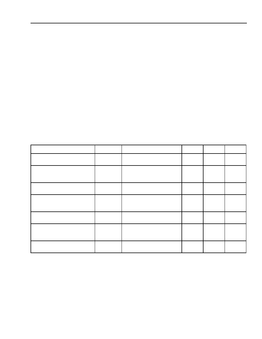
PCM Power Dissipation
Table 67. Programmable Clock Manager (PCM) Power Dissipation (Advance Information)
Parameter
Symbol
Test Conditions
Min
Max
Unit
Off State
PPCM_OFF
POWER_OFF = H,
no clock
—10
W
Maximum Power Dissipation in
PLL Mode
PMAX_PLL
POWER_OFF = L,
CLK_IN = 80 MHz,
PLL mode
—
100
mW
Standby Power Dissipation in
PLL Mode
PSTBY_PLL
POWER_OFF = L,
no clock, PLL mode
—10
mW
Maximum Power Dissipation in
DLL Mode
PMAX_DLL
POWER_OFF = L,
CLK_IN = 80 MHz,
DLL mode
—
100
mW
Standby Power Dissipation in
DLL Mode
PSTBY_DLL
POWER_OFF= L, no clock
DLL mode
—10
mW
Maximum Power Dissipation in
Clock 2x Mode
IMAX_CLK2x
POWER_OFF = L
CLK_IN = 80 MHz,
clock 2x mode
—
100
mW
Standby Power Dissipation in
Clock 2x Mode
ISTBY_CLK2x
POWER_OFF = L, no clock,
clock 2x mode
—10
mW
相關(guān)PDF資料 |
PDF描述 |
|---|---|
| OR3T165-4B600 | FPGA, 1024 CLBS, 120000 GATES, PBGA600 |
| OR3T165-4BA352I | FPGA, 1024 CLBS, 120000 GATES, PBGA352 |
| OR3T165-4BA352 | FPGA, 1024 CLBS, 120000 GATES, PBGA352 |
| OR3T165-4BC432I | FPGA, 1024 CLBS, 120000 GATES, PBGA432 |
| OR3T165-4BC600I | FPGA, 1024 CLBS, 120000 GATES, PBGA600 |
相關(guān)代理商/技術(shù)參數(shù) |
參數(shù)描述 |
|---|---|
| OR3T20 | 制造商:AGERE 制造商全稱:AGERE 功能描述:3C and 3T Field-Programmable Gate Arrays |
| OR3T20-4BA256I | 制造商:未知廠家 制造商全稱:未知廠家 功能描述:Field Programmable Gate Array (FPGA) |
| OR3T20-4S208I | 制造商:未知廠家 制造商全稱:未知廠家 功能描述:Field Programmable Gate Array (FPGA) |
| OR3T20-4S240I | 制造商:未知廠家 制造商全稱:未知廠家 功能描述:Field Programmable Gate Array (FPGA) |
| OR3T20-5BA256 | 制造商:AGERE 制造商全稱:AGERE 功能描述:3C and 3T Field-Programmable Gate Arrays |
發(fā)布緊急采購,3分鐘左右您將得到回復(fù)。