- 您現(xiàn)在的位置:買賣IC網(wǎng) > PDF目錄383706 > OR2T04A-3PS160 (Electronic Theatre Controls, Inc.) Field-Programmable Gate Arrays PDF資料下載
參數(shù)資料
| 型號: | OR2T04A-3PS160 |
| 廠商: | Electronic Theatre Controls, Inc. |
| 元件分類: | FPGA |
| 英文描述: | Field-Programmable Gate Arrays |
| 中文描述: | 現(xiàn)場可編程門陣列 |
| 文件頁數(shù): | 26/192頁 |
| 文件大小: | 3148K |
| 代理商: | OR2T04A-3PS160 |
第1頁第2頁第3頁第4頁第5頁第6頁第7頁第8頁第9頁第10頁第11頁第12頁第13頁第14頁第15頁第16頁第17頁第18頁第19頁第20頁第21頁第22頁第23頁第24頁第25頁當(dāng)前第26頁第27頁第28頁第29頁第30頁第31頁第32頁第33頁第34頁第35頁第36頁第37頁第38頁第39頁第40頁第41頁第42頁第43頁第44頁第45頁第46頁第47頁第48頁第49頁第50頁第51頁第52頁第53頁第54頁第55頁第56頁第57頁第58頁第59頁第60頁第61頁第62頁第63頁第64頁第65頁第66頁第67頁第68頁第69頁第70頁第71頁第72頁第73頁第74頁第75頁第76頁第77頁第78頁第79頁第80頁第81頁第82頁第83頁第84頁第85頁第86頁第87頁第88頁第89頁第90頁第91頁第92頁第93頁第94頁第95頁第96頁第97頁第98頁第99頁第100頁第101頁第102頁第103頁第104頁第105頁第106頁第107頁第108頁第109頁第110頁第111頁第112頁第113頁第114頁第115頁第116頁第117頁第118頁第119頁第120頁第121頁第122頁第123頁第124頁第125頁第126頁第127頁第128頁第129頁第130頁第131頁第132頁第133頁第134頁第135頁第136頁第137頁第138頁第139頁第140頁第141頁第142頁第143頁第144頁第145頁第146頁第147頁第148頁第149頁第150頁第151頁第152頁第153頁第154頁第155頁第156頁第157頁第158頁第159頁第160頁第161頁第162頁第163頁第164頁第165頁第166頁第167頁第168頁第169頁第170頁第171頁第172頁第173頁第174頁第175頁第176頁第177頁第178頁第179頁第180頁第181頁第182頁第183頁第184頁第185頁第186頁第187頁第188頁第189頁第190頁第191頁第192頁
26
Lucent Technologies Inc.
Data Sheet
June 1999
ORCA Series 2 FPGAs
Programmable Input/Output Cells
(continued)
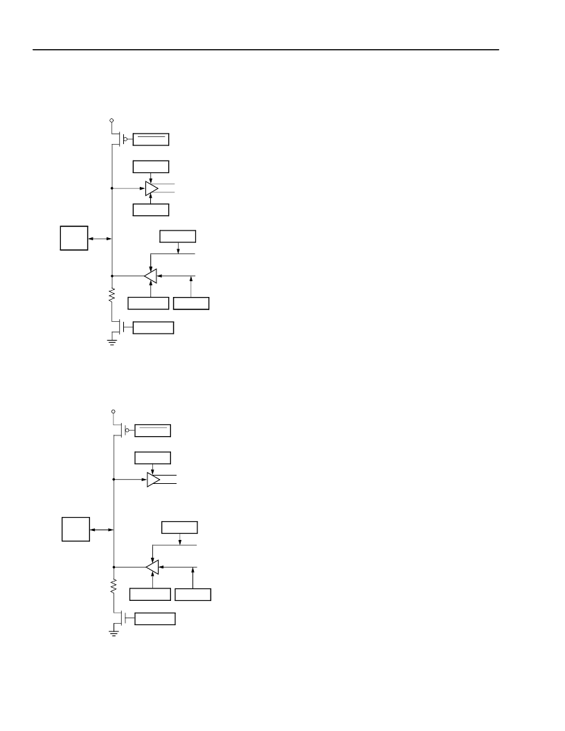
A. Simplified Diagram of OR2CxxA Programmable
I/O Cell (PIC)
B. Simplified Diagram of OR2TxxA/OR2TxxB
Programmable I/O Cell (PIC)
Figure 24. Simplified Diagrams
Outputs
The PIC’s output drivers have programmable drive
capability and slew rates. Three propagation delays
(fast, slewlim, sinklim) are available on output drivers.
The sinklim mode has the longest propagation delay
and is used to minimize system noise and minimize
power consumption. The fast and slewlim modes allow
critical timing to be met.
The drive current is 12 mA sink/6 mA source for the
slewlim and fast output speed selections and
6 mA sink/3 mA source for the sinklim output. Two adja-
cent outputs can be interconnected to increase the out-
put sink current to 24 mA.
All outputs that are not speed critical should be config-
ured as sinklim to minimize power and noise. The num-
ber of outputs that switch simultaneously in the same
direction should be limited to minimize ground bounce.
To minimize ground bounce problems, locate heavily
loaded output buffers near the ground pads. Ground
bounce is generally a function of the driving circuits,
traces on the PCB, and loads and is best determined
with a circuit simulation.
Outputs can be inverted, and 3-state control signals
can be active-high or active-low. An open-drain output
may be obtained by using the same signal for driving
the output and 3-state signal nets so that the buffer out-
put is enabled only by a low. At powerup, the output
drivers are in slewlim mode, and the input buffers are
configured as TTL-level compatible with a pull-up. If an
output is not to be driven in the selected configuration
mode, it is 3-stated.
5 V Tolerant I/O (OR2TxxA)
The I/O on the OR2TxxA series devices allow intercon-
nection to both 3.3 V and 5 V device (selectable on a
per-pin basis) by way of special V
DD
5 pins that have
been added to the OR2TxxA devices. If any I/O on the
OR2TxxA device interfaces to a 5 V input, then all of
the V
DD
5 pins must be connected to the 5 V supply. If
no pins on the device interface to a 5 V signal, then the
V
DD
5 pins must be connected to the 3.3 V supply.
If the V
DD
5 pins are disconnected (i.e., they are float-
ing), the device will not be damaged; however, the
device may not operate properly until V
DD
5 is returned
to a proper voltage level. If the V
DD
5 pins are then
shorted to ground, a large current flow will develop, and
the device may be damaged.
PULL-UP
V
DD
DELAY
TTL/CMOS
PAD
SLEW RATE
POLARITY
DOUT/OUT
PULL-DOWN
dintb, dinlr
in
POLARITY
TRI
5-4591(F)
PULL-UP
V
DD
DELAY
PAD
SLEW RATE
POLARITY
DOUT/OUT
PULL-DOWN
dintb, dinlr
in
POLARITY
TRI
5-4591.T(F)
相關(guān)PDF資料 |
PDF描述 |
|---|---|
| OR2T04A-3PS160I | Field-Programmable Gate Arrays |
| OR2C40A-3S304 | Field-Programmable Gate Arrays |
| OR2C40A-3T304 | Field-Programmable Gate Arrays |
| OR2C40A-3T304I | Field-Programmable Gate Arrays |
| OR2C40A-3T432 | Field-Programmable Gate Arrays |
相關(guān)代理商/技術(shù)參數(shù) |
參數(shù)描述 |
|---|---|
| OR2T04A-3PS160I | 制造商:未知廠家 制造商全稱:未知廠家 功能描述:Field-Programmable Gate Arrays |
| OR2T04A-3PS208 | 制造商:未知廠家 制造商全稱:未知廠家 功能描述:Field-Programmable Gate Arrays |
| OR2T04A-3PS208I | 制造商:未知廠家 制造商全稱:未知廠家 功能描述:Field-Programmable Gate Arrays |
| OR2T04A-3PS84 | 制造商:未知廠家 制造商全稱:未知廠家 功能描述:Field-Programmable Gate Arrays |
| OR2T04A-3PS84I | 制造商:未知廠家 制造商全稱:未知廠家 功能描述:Field-Programmable Gate Arrays |
發(fā)布緊急采購,3分鐘左右您將得到回復(fù)。