- 您現(xiàn)在的位置:買賣IC網(wǎng) > PDF目錄224638 > OR2C15A-2M352 (Electronic Theatre Controls, Inc.) Field-Programmable Gate Arrays PDF資料下載
參數(shù)資料
| 型號(hào): | OR2C15A-2M352 |
| 廠商: | Electronic Theatre Controls, Inc. |
| 元件分類: | FPGA |
| 英文描述: | Field-Programmable Gate Arrays |
| 中文描述: | 現(xiàn)場(chǎng)可編程門陣列 |
| 文件頁數(shù): | 150/192頁 |
| 文件大小: | 3148K |
| 代理商: | OR2C15A-2M352 |
第1頁第2頁第3頁第4頁第5頁第6頁第7頁第8頁第9頁第10頁第11頁第12頁第13頁第14頁第15頁第16頁第17頁第18頁第19頁第20頁第21頁第22頁第23頁第24頁第25頁第26頁第27頁第28頁第29頁第30頁第31頁第32頁第33頁第34頁第35頁第36頁第37頁第38頁第39頁第40頁第41頁第42頁第43頁第44頁第45頁第46頁第47頁第48頁第49頁第50頁第51頁第52頁第53頁第54頁第55頁第56頁第57頁第58頁第59頁第60頁第61頁第62頁第63頁第64頁第65頁第66頁第67頁第68頁第69頁第70頁第71頁第72頁第73頁第74頁第75頁第76頁第77頁第78頁第79頁第80頁第81頁第82頁第83頁第84頁第85頁第86頁第87頁第88頁第89頁第90頁第91頁第92頁第93頁第94頁第95頁第96頁第97頁第98頁第99頁第100頁第101頁第102頁第103頁第104頁第105頁第106頁第107頁第108頁第109頁第110頁第111頁第112頁第113頁第114頁第115頁第116頁第117頁第118頁第119頁第120頁第121頁第122頁第123頁第124頁第125頁第126頁第127頁第128頁第129頁第130頁第131頁第132頁第133頁第134頁第135頁第136頁第137頁第138頁第139頁第140頁第141頁第142頁第143頁第144頁第145頁第146頁第147頁第148頁第149頁當(dāng)前第150頁第151頁第152頁第153頁第154頁第155頁第156頁第157頁第158頁第159頁第160頁第161頁第162頁第163頁第164頁第165頁第166頁第167頁第168頁第169頁第170頁第171頁第172頁第173頁第174頁第175頁第176頁第177頁第178頁第179頁第180頁第181頁第182頁第183頁第184頁第185頁第186頁第187頁第188頁第189頁第190頁第191頁第192頁
60
Lucent Technologies Inc.
Data Sheet
ORCA Series 2 FPGAs
June 1999
ORCA Timing Characteristics
To define speed grades, the
ORCA Series part number
designation (see Table 54) uses a single-digit number
to designate a speed grade. This number is not related
to any single ac parameter. Higher numbers indicate a
faster set of timing parameters. The actual speed sort-
ing is based on testing the delay in a path consisting of
an input buffer, combinatorial delay through all PLCs in
a row, and an output buffer. Other tests are then done
to verify other delay parameters, such as routing
delays, setup times to FFs, etc.
The most accurate timing characteristics are reported
by the timing analyzer in the
ORCA Foundry Develop-
ment System. A timing report provided by the develop-
ment system after layout divides path delays into logic
and routing delays. The timing analyzer can also pro-
vide logic delays prior to layout. While this allows rout-
ing budget estimates, there is wide variance in routing
delays associated with different layouts.
The logic timing parameters noted in the Electrical
Characteristics section of this data sheet are the same
as those in the design tools. In the PFU timing given in
Tables 31—79, symbol names are generally a concate-
nation of the PFU operating mode (as defined in
Table 3) and the parameter type. The wildcard charac-
ter (*) is used in symbol names to indicate that the
parameter applies to any sub-LUT. The setup, hold,
and propagation delay parameters, defined below, are
designated in the symbol name by the SET, HLD, and
DEL characters, respectively.
The values given for the parameters are the same as
those used during production testing and speed bin-
ning of the devices. The junction temperature and sup-
ply voltage used to characterize the devices are listed
in the delay tables. Actual delays at nominal tempera-
ture and voltage for best-case processes can be much
better than the values given.
It should be noted that the junction temperature used in
the tables is generally 85 °C. The junction temperature
for the FPGA depends on the power dissipated by the
device, the package thermal characteristics (
ΘJA), and
the ambient temperature, as calculated in the following
equation and as discussed further in the Package
Thermal Characteristics section:
TJmax = TAmax + (P
ΘJA) °C
Note: The user must determine this junction tempera-
ture to see if the delays from
ORCA Foundry
should be derated based on the following derat-
ing tables.
Table 14A and 14B and provide approximate power
supply and junction temperature derating for OR2CxxA
commercial and industrial devices. Table 15A and 15B
provides the same information for the OR2TxxA and
OR2TxxB devices (both commercial and industrial).
The delay values in this data sheet and reported by
ORCA Foundry are shown as 1.00 in the tables. The
method for determining the maximum junction temper-
ature is defined in the Thermal Characteristics section.
Taken cumulatively, the range of parameter values for
best-case vs. worst-case processing, supply voltage,
and junction temperature can approach 3 to 1.
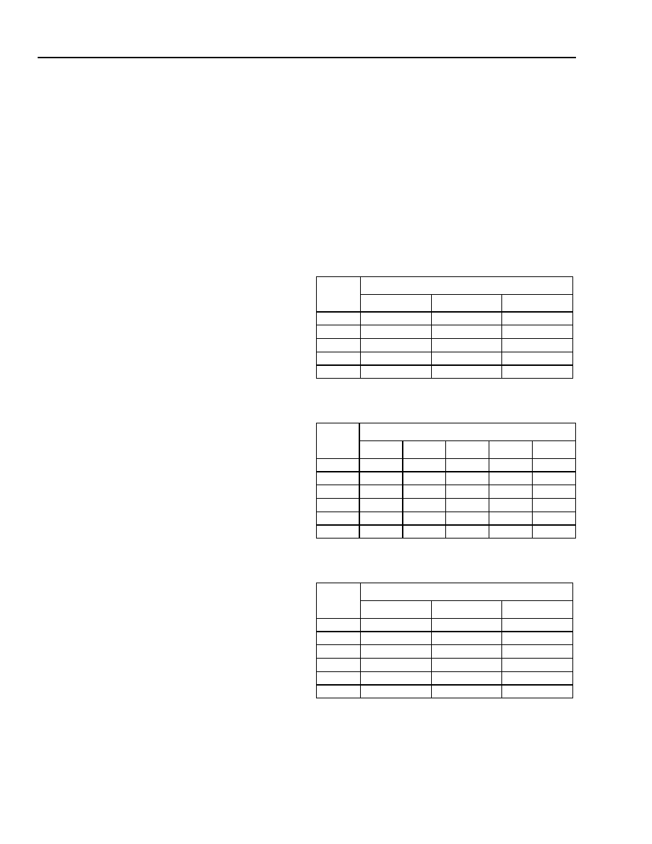
Table 14A. Derating for Commercial Devices
(OR2CxxA)
Table 14B. Derating for Industrial Devices
(OR2CxxA)
Table 15A. Derating for Commercial/Industrial
Devices (OR2TxxA)
TJ
(°C)
Power Supply Voltage
4.75 V
5.0 V
5.25 V
0
0.81
0.79
0.77
25
0.85
0.83
0.81
85
1.00
0.97
0.95
100
1.05
1.02
1.00
125
1.12
1.09
1.07
TJ
(°C)
Power Supply Voltage
4.5 V
4.75 V
5.0 V
5.25 V
5.5 V
–40
0.71
0.70
0.68
0.66
0.65
0
0.80
0.78
0.76
0.74
0.73
25
0.84
0.82
0.80
0.78
0.77
85
1.00
0.97
0.94
0.93
0.91
100
1.05
1.01
0.99
0.97
0.95
125
1.12
1.09
1.06
1.04
1.02
TJ
(°C)
Power Supply Voltage
3.0 V
3.3 V
3.6 V
–40
0.73
0.66
0.61
0
0.82
0.73
0.68
25
0.87
0.78
0.72
85
1.00
0.90
0.83
100
1.04
0.94
0.87
125
1.10
1.00
0.92
相關(guān)PDF資料 |
PDF描述 |
|---|---|
| OR2C15A-2M352I | Field-Programmable Gate Arrays |
| OR2C15A-2M432 | Field-Programmable Gate Arrays |
| OR2C15A-2M432I | Field-Programmable Gate Arrays |
| OR2C15A-2M84 | Field-Programmable Gate Arrays |
| OR2C15A-2M84I | Field-Programmable Gate Arrays |
相關(guān)代理商/技術(shù)參數(shù) |
參數(shù)描述 |
|---|---|
| OR2C15A3BA256I-DB | 功能描述:FPGA - 現(xiàn)場(chǎng)可編程門陣列 1600 LUT 298 I/O RoHS:否 制造商:Altera Corporation 系列:Cyclone V E 柵極數(shù)量: 邏輯塊數(shù)量:943 內(nèi)嵌式塊RAM - EBR:1956 kbit 輸入/輸出端數(shù)量:128 最大工作頻率:800 MHz 工作電源電壓:1.1 V 最大工作溫度:+ 70 C 安裝風(fēng)格:SMD/SMT 封裝 / 箱體:FBGA-256 |
| OR2C15A3BA352I-DB | 功能描述:FPGA - 現(xiàn)場(chǎng)可編程門陣列 Use ECP/EC or XP RoHS:否 制造商:Altera Corporation 系列:Cyclone V E 柵極數(shù)量: 邏輯塊數(shù)量:943 內(nèi)嵌式塊RAM - EBR:1956 kbit 輸入/輸出端數(shù)量:128 最大工作頻率:800 MHz 工作電源電壓:1.1 V 最大工作溫度:+ 70 C 安裝風(fēng)格:SMD/SMT 封裝 / 箱體:FBGA-256 |
| OR2C15A3M84I-D | 功能描述:FPGA - 現(xiàn)場(chǎng)可編程門陣列 1600 LUT 298 I/O RoHS:否 制造商:Altera Corporation 系列:Cyclone V E 柵極數(shù)量: 邏輯塊數(shù)量:943 內(nèi)嵌式塊RAM - EBR:1956 kbit 輸入/輸出端數(shù)量:128 最大工作頻率:800 MHz 工作電源電壓:1.1 V 最大工作溫度:+ 70 C 安裝風(fēng)格:SMD/SMT 封裝 / 箱體:FBGA-256 |
| OR2C15A3PS208I-DB | 功能描述:FPGA - 現(xiàn)場(chǎng)可編程門陣列 1600 LUT 298 I/O RoHS:否 制造商:Altera Corporation 系列:Cyclone V E 柵極數(shù)量: 邏輯塊數(shù)量:943 內(nèi)嵌式塊RAM - EBR:1956 kbit 輸入/輸出端數(shù)量:128 最大工作頻率:800 MHz 工作電源電壓:1.1 V 最大工作溫度:+ 70 C 安裝風(fēng)格:SMD/SMT 封裝 / 箱體:FBGA-256 |
| OR2C15A3PS240I-DB | 功能描述:FPGA - 現(xiàn)場(chǎng)可編程門陣列 1600 LUT 298 I/O RoHS:否 制造商:Altera Corporation 系列:Cyclone V E 柵極數(shù)量: 邏輯塊數(shù)量:943 內(nèi)嵌式塊RAM - EBR:1956 kbit 輸入/輸出端數(shù)量:128 最大工作頻率:800 MHz 工作電源電壓:1.1 V 最大工作溫度:+ 70 C 安裝風(fēng)格:SMD/SMT 封裝 / 箱體:FBGA-256 |
發(fā)布緊急采購,3分鐘左右您將得到回復(fù)。