- 您現(xiàn)在的位置:買賣IC網(wǎng) > PDF目錄376244 > OP295 (Analog Devices, Inc.) DUAL/QUAD RAIL-TO-RAIL OPERATIONAL AMPLIFIERS PDF資料下載
參數(shù)資料
| 型號: | OP295 |
| 廠商: | Analog Devices, Inc. |
| 英文描述: | DUAL/QUAD RAIL-TO-RAIL OPERATIONAL AMPLIFIERS |
| 中文描述: | 雙/四軌至軌運算放大器 |
| 文件頁數(shù): | 8/12頁 |
| 文件大小: | 328K |
| 代理商: | OP295 |
REV. B
–8–
OP295/OP495
T able I. Single Supply Low Noise Preamp Performance
I
C
= 1.85 mA
I
C
= 0.5 mA
R1
R3, R4
e
n
@ 100 Hz
e
n
@ 10 Hz
I
SY
I
B
Bandwidth
Closed-Loop Gain
270
200
3.15 nV/
√
Hz
4.2 nV/
√
Hz
4.0 mA
11
μ
A
1 kHz
1000
1.0 k
910
8.6 nV/
√
Hz
10.2 nV/
√
Hz
1.3 mA
3
μ
A
1 kHz
1000
Driving Heavy Loads
T he OP295/OP495 is well suited to drive loads by using a
power transistor, Darlington or FET to increase the current to
the load. T he ability to swing to either rail can assure that the
device is turned on hard. T his results in more power to the load
and an increase in efficiency over using standard op amps with
their limited output swing. Driving power FET s is also possible
with the OP295/OP495 because of its ability to drive capacitive
loads of several hundred picofarads without oscillating.
Without the addition of external transistors the OP295/OP495
can drive loads in excess of
±
15 mA with
±
15 or +30 volt
supplies. T his drive capability is somewhat decreased at lower
supply voltages. At
±
5 volt supplies the drive current is
±
11 mA.
Driving motors or actuators in two directions in a single supply
application is often accomplished using an “H” bridge. T he
principle is demonstrated in Figure 3a. From a single +5 volt
supply this driver is capable of driving loads from 0.8 V to 4.2 V
in both directions. Figure 3b shows the voltages at the inverting
and noninverting outputs of the driver. T here is a small crossover
glitch that is frequency dependent and would not cause problems
5k
10k
1.67V
10k
10k
2N2222
2N2222
OUTPUTS
2N2907
2N2907
+5V
0
≤
V
IN
≤
2.5V
Figure 3a. “ H” Bridge
10
90
100
0%
2V
2V
1ms
Figure 3b. “ H” Bridge Outputs
unless this was a low distortion application such as audio. If this
is used to drive inductive loads, be sure to add diode clamps to
protect the bridge from inductive kickback.
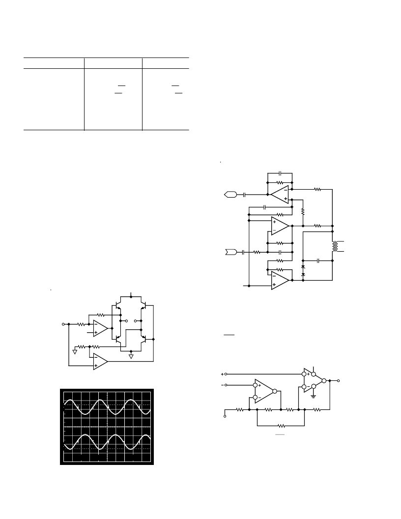
Direct Access Arrangement
OP295/OP495 can be used in a single supply Direct Access Ar-
rangement (DAA) as is shown an in Figure 4. T his figure shows
a portion of a typical DM capable of operating from a single
+5 volt supply and it may also work on +3 volt supplies with
minor modifications. Amplifiers A2 and A3 are configured so
that the transmit signal T X A is inverted by A2 and is not in-
verted by A3. T his arrangement drives the transformer differen-
tially so that the drive to the transformer is effectively doubled
over a single amplifier arrangement. T his application takes ad-
vantage of the OP295/OP495’s ability to drive capacitive loads,
and to save power in single supply applications.
2.5V REF
A3
20k
20k
750pF
20k
22.1k
0.1
μ
F
475
3.3k
0.0047
μ
F
0.1
μ
F
0.033
μ
F
A2
A1
20k
20k
37.4k
390pF
RXA
TXA
OP295/
OP495
OP295/
OP495
OP295/
OP495
1:1
Figure 4. Direct Access Arrangement
A Single Supply Instrumentation Amplifier
T he OP295/OP495 can be configured as a single supply instru-
mentation amplifier as in Figure 5. For our example, V
REF
is set
V
+
2
put common-mode voltage range includes ground and the out-
put swings to both rails.
equal to
and V
O
is measured with respect to V
REF
. T he in-
V+
V
IN
V
REF
1
R1
100k
R2
20k
R3
20k
R4
100k
V
O
V
IN
+ V
REF
V
O
= 5 +R
G
)
R
G
3
2
8
7
4
5
6
1/2
OP295/
OP495
1/2
OP295/
OP495
Figure 5. Single Supply Instrumentation Amplifier
Resistor R
G
sets the gain of the instrumentation amplifier. Mini-
mum gain is 6 (with no R
G
). All resistors should be matched in
absolute value as well as temperature coefficient to maximize
相關(guān)PDF資料 |
PDF描述 |
|---|---|
| OP295GP | DUAL/QUAD RAIL-TO-RAIL OPERATIONAL AMPLIFIERS |
| OP495GP | DUAL/QUAD RAIL-TO-RAIL OPERATIONAL AMPLIFIERS |
| OP295GS | DUAL/QUAD RAIL-TO-RAIL OPERATIONAL AMPLIFIERS |
| OP495GS | DUAL/QUAD RAIL-TO-RAIL OPERATIONAL AMPLIFIERS |
| op295 | Rail to Rail Dual OP AMP(滿幅度雙運算放大器) |
相關(guān)代理商/技術(shù)參數(shù) |
參數(shù)描述 |
|---|---|
| OP295_06 | 制造商:AD 制造商全稱:Analog Devices 功能描述:Dual/Quad Rail-to-Rail Operational Amplifiers |
| OP2950013P | 制造商:Rochester Electronics LLC 功能描述:- Bulk |
| OP295A | 功能描述:紅外發(fā)射源 Infrared 890nm RoHS:否 制造商:Fairchild Semiconductor 波長:880 nm 射束角:+/- 25 輻射強度: 最大工作溫度:+ 100 C 最小工作溫度:- 40 C 封裝 / 箱體:Side Looker 封裝:Bulk |
| OP295AZ/883 | 制造商:未知廠家 制造商全稱:未知廠家 功能描述:Voltage-Feedback Operational Amplifier |
| OP295B | 功能描述:紅外發(fā)射源 Infrared 890nm RoHS:否 制造商:Fairchild Semiconductor 波長:880 nm 射束角:+/- 25 輻射強度: 最大工作溫度:+ 100 C 最小工作溫度:- 40 C 封裝 / 箱體:Side Looker 封裝:Bulk |
發(fā)布緊急采購,3分鐘左右您將得到回復。