- 您現(xiàn)在的位置:買賣IC網(wǎng) > PDF目錄359740 > NJU26105 (New Japan Radio Co., Ltd.) NJU26100 Series Hardware Specification PDF資料下載
參數(shù)資料
| 型號: | NJU26105 |
| 廠商: | New Japan Radio Co., Ltd. |
| 英文描述: | NJU26100 Series Hardware Specification |
| 中文描述: | NJU26100系列硬件規(guī)格 |
| 文件頁數(shù): | 15/17頁 |
| 文件大?。?/td> | 270K |
| 代理商: | NJU26105 |
Ver.2005-02-24
NJU26100 Series
- 15 -
5.2 I
2
C Bus
When the NJU26100 Series is configured for I
2
C bus communication in GPIO0 pin (*SEL1 pin)=”Low”, the serial
host interface transfers data to the SDA pin and clocks data to the SCL pin. SDA is an open drain pin requiring an
external 4.7k pull-up resistor. AD1 and AD2 pins are used to configure the seven-bit SLAVE address of the serial
host interface. This offers additional flexibility to a system design by four different SLAVE addresses of the
NJU26100 Series. An address can be arbitrarily set up by the AD1, 2 pins. The I
2
C address of AD1, 2 is decided by
connection of AD1, 2 pins. The I
2
C address should be the same level of AD1, 2 pins. The real I
2
C address is
described in the each data sheet. Refer to the each data sheet.
* It excepts NJU26150. Refer to each data sheet.
Table 5-3 I
2
C Bus SLAVE Address
bit7
bit6
bit5
bit4
bit3
0
0
1
1
1
*1 The SLAVE address bit is 0 when ADx-pin is low level. The SLAVE address bit is 1 when ADx-pin is high level.
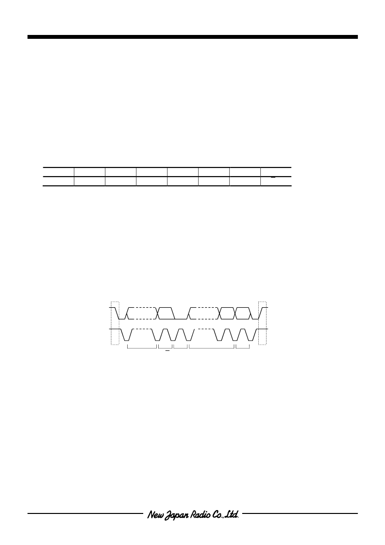
The figure on the following page shows the basic timing relationships for transfers. A transfer is initiated with a
START condition, followed by the SLAVE address byte. The SLAVE address consists of the seven-bit SLAVE
address followed by a read/write (R/W) bit. When an address with an effective serial host interface is detected, the
acknowledgement bit which sets a SDA line to Low in the ninth bit clock cycle is returned.
The R/W bit in the SLAVE address byte sets the direction of data transmission until a STOP condition terminates
the transfer. R/W = 0 indicates the host will send to the NJU26100 Series while R/W = 1 indicates the host will
receive data from the NJU26100 Series.
bit2
AD2*
1
bit1
AD1*
1
bit0
R/W
Fig. 5-2 I
2
C Bus Format
In case of the NJU26100 Series, only single-byte transmission is available.
The serial host interface supports “Standard-Mode (100kbps)” I
2
C bus data transfer.
1-7
8
9
1-7
8
9
S
P
SDA
SCL
Address
Data
ACK
ACK
R/W
Start
Stop
相關(guān)PDF資料 |
PDF描述 |
|---|---|
| NJU26106 | NJU26100 Series Hardware Specification |
| NJU26107 | NJU26100 Series Hardware Specification |
| NJU26109 | NJU26100 Series Hardware Specification |
| NJU26110 | NJU26100 Series Hardware Specification |
| NJU26111 | NJU26100 Series Hardware Specification |
相關(guān)代理商/技術(shù)參數(shù) |
參數(shù)描述 |
|---|---|
| NJU26105FR1 | 功能描述:數(shù)字信號處理器和控制器 - DSP, DSC EALA 3.1 ch Output Digtl Signl Processr RoHS:否 制造商:Microchip Technology 核心:dsPIC 數(shù)據(jù)總線寬度:16 bit 程序存儲器大小:16 KB 數(shù)據(jù) RAM 大小:2 KB 最大時鐘頻率:40 MHz 可編程輸入/輸出端數(shù)量:35 定時器數(shù)量:3 設(shè)備每秒兆指令數(shù):50 MIPs 工作電源電壓:3.3 V 最大工作溫度:+ 85 C 封裝 / 箱體:TQFP-44 安裝風(fēng)格:SMD/SMT |
| NJU26106 | 制造商:NJRC 制造商全稱:New Japan Radio 功能描述:NJU26100 Series Hardware Specification |
| NJU26106FR1 | 制造商:New Japan Radio Co Ltd (NJR/JRC) 功能描述:SPECIALTY CONSUMER CIRCUIT, 32 Pin Plastic QFP |
| NJU26107 | 制造商:NJRC 制造商全稱:New Japan Radio 功能描述:NJU26100 Series Hardware Specification |
| NJU26108 | 制造商:NJRC 制造商全稱:New Japan Radio 功能描述:NJU26100 Series Hardware Specification |
發(fā)布緊急采購,3分鐘左右您將得到回復(fù)。