- 您現(xiàn)在的位置:買賣IC網(wǎng) > PDF目錄361102 > NCP5210MNR2G (ON SEMICONDUCTOR) 3-in-1 PWM Dual Buck and Linear DDR Power Controller PDF資料下載
參數(shù)資料
| 型號: | NCP5210MNR2G |
| 廠商: | ON SEMICONDUCTOR |
| 元件分類: | 穩(wěn)壓器 |
| 英文描述: | 3-in-1 PWM Dual Buck and Linear DDR Power Controller |
| 中文描述: | DUAL SWITCHING CONTROLLER, 550 kHz SWITCHING FREQ-MAX, PDSO20 |
| 封裝: | 6 X 5 MM, LEAD FREE, PLASTIC, QFN-20 |
| 文件頁數(shù): | 4/18頁 |
| 文件大小: | 183K |
| 代理商: | NCP5210MNR2G |
NCP5210
http://onsemi.com
4
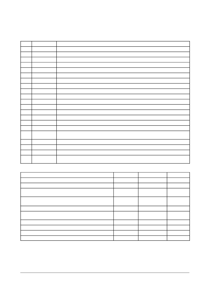
PIN DESCRIPTION
Pin
Symbol
Description
1
COMP
VDDQ error amplifier compensation node.
2
FBDDQ
DDQ regulator feedback pin.
3
SS
Softstart pin of DDQ and MCH.
4
PGND
Power ground.
5
VTT
VTT regulator output.
6
VDDQ
Power input for VTT linear regulator.
7
AGND
Analog ground connection and remote ground sense.
8
FBVTT
VTT regulator pin for closed loop regulation.
9
DDQ_REF
Reference voltage input of VTT regulator.
10
FB1P5
V1P5 switching regulator feedback pin.
11
GND_1P5
Power ground for V1P5 regulator.
12
BG_1P5
Gate driver output for V1P5 regulator low side NChannel Power FET.
13
TG_1P5
Gate driver output for V1P5 regulator high side NChannel Power FET.
14
BUF_Cut
Active HIGH control signal to activate S3 sleep state.
15
COMP_1P5
V1P5 error amplifier compensation node.
16
5VDUAL
5.0 V Dual supply input, which is monitored by undervoltage lock out circuitry.
17
BOOT
Gate driver input supply, which is monitored by undervoltage lock out circuitry, and a boost capacitor
connection between SWDDQ and this pin.
18
TG_DDQ
Gate driver output for DDQ regulator high side NChannel Power FET.
19
BG_DDQ
Gate driver output for DDQ regulator low side NChannel Power FET.
20
SW_DDQ
DDQ regulator switch node and current limit sense input.
21
TH_PAD
Copper pad on bottom of IC used for heatsinking. This pin should be connected to the ground plane under
the IC.
MAXIMUM RATINGS
Rating
Symbol
Value
Unit
Power Supply Voltage (Pin 16) to AGND (Pin 7)
5VDUAL
0.3, 6.0
V
BOOT (Pin 17) to AGND (Pin 7)
BOOT
0.3, 14
V
Gate Drive (Pins 12, 13, 18, 19) to AGND (Pin 7)
Vg
0.3 DC,
100 ns; 14
4.0 for
V
Input / Output Pins to AGND (Pin 7)
Pins 13, 56, 810, 1415, 20
V
IO
0.3, 6.0
V
PGND (Pin 4), GND_1P5 (Pin 11) to AGND (Pin 7)
V
GND
0.3, 0.3
V
Thermal Characteristics, QFN20 Plastic Package
Thermal Resistance JunctiontoAir
R
JA
35
°
C/W
Operating Junction Temperature Range
T
J
0 to + 150
°
C
Operating Ambient Temperature Range
T
A
0 to + 70
°
C
Storage Temperature Range
T
stg
55 to +150
°
C
Moisture Sensitivity Level
Maximum ratings are those values beyond which device damage can occur. Maximum ratings applied to the device are individual stress limit
values (not normal operating conditions) and are not valid simultaneously. If these limits are exceeded, device functional operation is not implied,
damage may occur and reliability may be affected.
1. This device series contains ESD protection and exceeds the following tests: Human Body Model (HBM)
JESD22–A114. Machine Model (MM)
200 V per JEDEC standard: JESD22–A115.
2. Latchup Current Maximum Rating:
150 mA per JEDEC standard: JESD78.
MSL
2.0
2.0 kV per JEDEC standard:
相關(guān)PDF資料 |
PDF描述 |
|---|---|
| NCP5211BDR2G | Low Voltage Synchronous Buck Controller |
| NCP5211DR2G | Low Voltage Synchronous Buck Controller |
| NCP5214A | 2−in−1 Notebook DDR Power Controller |
| NCP5214AMNR2G | 2−in−1 Notebook DDR Power Controller |
| NCP5214 | 2-in-1 Notebook DDR Power Controller |
相關(guān)代理商/技術(shù)參數(shù) |
參數(shù)描述 |
|---|---|
| NCP5211 | 制造商:ONSEMI 制造商全稱:ON Semiconductor 功能描述:Low Voltage Synchronous Buck Controller |
| NCP5211A | 制造商:ONSEMI 制造商全稱:ON Semiconductor 功能描述:Low Voltage Synchronous Buck Controller |
| NCP5211A/D | 制造商:未知廠家 制造商全稱:未知廠家 功能描述:Low Voltage Synchronous Buck Controller |
| NCP5211AD | 制造商:ONSEMI 制造商全稱:ON Semiconductor 功能描述:Low Voltage Synchronous Buck Controller |
| NCP5211ADR2 | 功能描述:IC REG CTRLR BUCK PWM 14-SOIC RoHS:否 類別:集成電路 (IC) >> PMIC - 穩(wěn)壓器 - DC DC 切換控制器 系列:- 標(biāo)準(zhǔn)包裝:4,000 系列:- PWM 型:電壓模式 輸出數(shù):1 頻率 - 最大:1.5MHz 占空比:66.7% 電源電壓:4.75 V ~ 5.25 V 降壓:是 升壓:無 回掃:無 反相:無 倍增器:無 除法器:無 Cuk:無 隔離:無 工作溫度:-40°C ~ 85°C 封裝/外殼:40-VFQFN 裸露焊盤 包裝:帶卷 (TR) |
發(fā)布緊急采購,3分鐘左右您將得到回復(fù)。