- 您現(xiàn)在的位置:買賣IC網(wǎng) > PDF目錄1956 > NCN4557MTG (ON Semiconductor)IC SMART CARD/SIM DUAL 16-QFN PDF資料下載
參數(shù)資料
| 型號: | NCN4557MTG |
| 廠商: | ON Semiconductor |
| 文件頁數(shù): | 9/12頁 |
| 文件大小: | 0K |
| 描述: | IC SMART CARD/SIM DUAL 16-QFN |
| 產(chǎn)品變化通告: | Product Discontinuation 30/Sept/2011 |
| 標準包裝: | 123 |
| 系列: | * |
| 應用: | * |
| 接口: | * |
| 電源電壓: | * |
| 封裝/外殼: | 16-WFQFN 裸露焊盤 |
| 供應商設備封裝: | 16-QFN(3x3) |
| 包裝: | 管件 |
| 安裝類型: | 表面貼裝 |
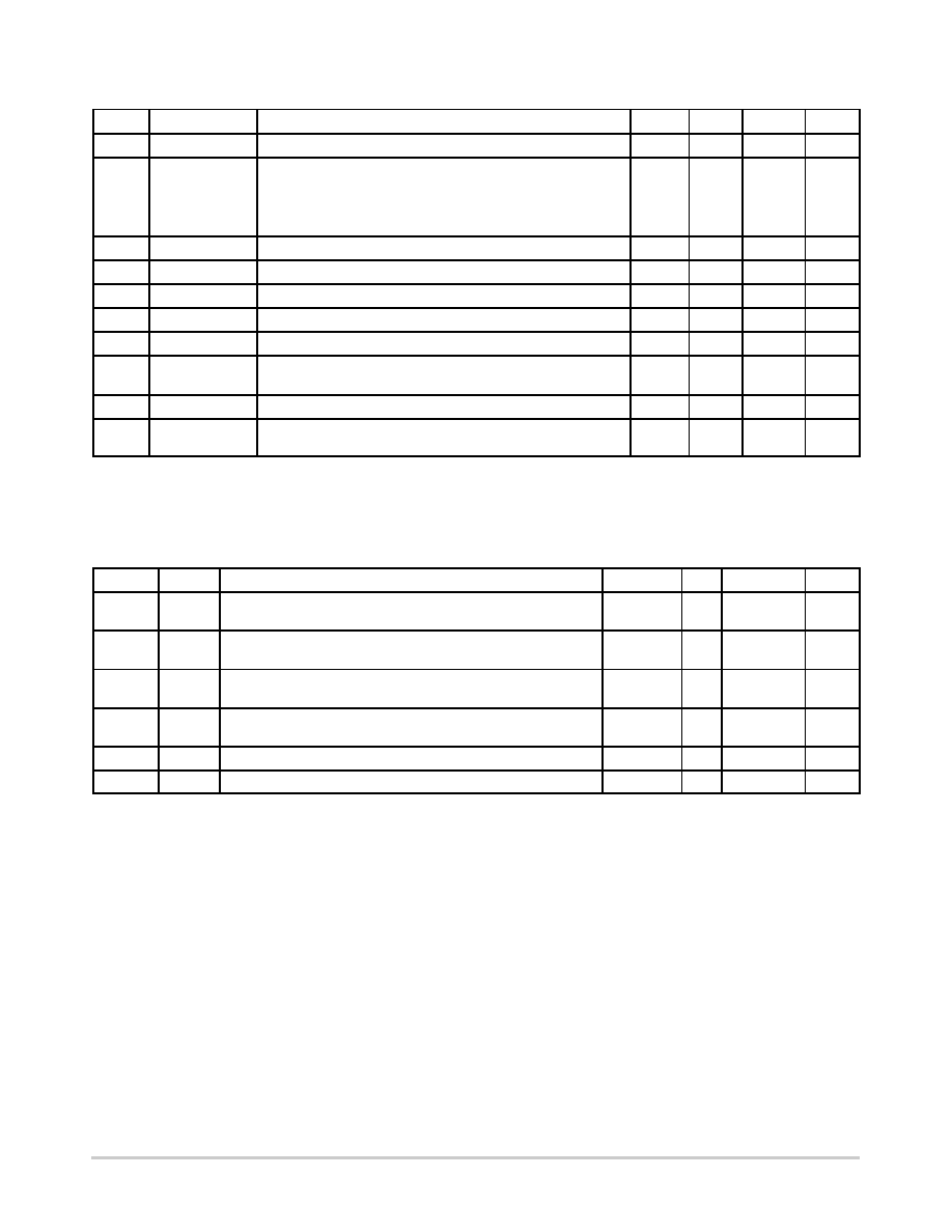
NCN4557
http://onsemi.com
6
POWER SUPPLY SECTION (40
°C to +85°C)
Pin
Symbol
Rating
Min
Typ
Max
Unit
3
VBAT
Power Supply
2.7
5.5
V
3
IVBAT
Operating current
CRD_VCCA = 3.0 V, CRD_VCCB = 0 V, ICCA & B = 0 mA
CRD_VCCA = 1.8 V, CRD_VCCB = 0 V, ICCA & B = 0 mA
CRD_VCCA = 0 V, CRD_VCCB = 3.0 V, ICCA & B = 0 mA
CRD_VCCA = 0 V, CRD_VCCB = 1.8 V, ICCA & B = 0 mA
26
25
26
25
80
mA
3
IVBAT_SD
Shutdown current – ENABLE = Low
3
mA
2
VDD
Operating Voltage
1.8
5.5
V
2
IVDD
Operating Current (CLK & RST Low)
0.1
2
mA
2
IVDD_SD
Shutdown Current – ENABLE = Low
0.05
1
mA
2
VDD
Undervoltage Lockout
0.6
1.5
V
1,4
CRD_VCCA or B
3.0 V Mode, VBAT = 3.3 V to 5.5 V, ICRD_VCC = 0 mA to 50 mA
1.8 V Mode, VBAT = 2.7 V to 5.5 V, ICRD_VCC = 0 mA to 50 mA
2.75
1.65
3.0
1.8
3.25
1.95
V
1,4
ICRD_VCC_SC
Short –Circuit Current – CRD_VCC Shorted to GND, TA = 25°C
50
175
mA
7,13,14
Channel Turnon Time
ICCA or B = 0 mA, ENABLE rise edge to CRD_I/OA or B rise edge
0.8
2.5
ms
NOTE: Device will meet the specifications after thermal equilibrium has been established when mounted in a test socket or printed circuit
board with maintained transverse airflow greater than 500 lfpm. Electrical parameters are guaranteed only over the declared operating
temperature range. Functional operation of the device exceeding these conditions is not implied. Device specification limit values are
applied individually under normal operating conditions and not valid simultaneously.
DIGITAL INPUT/OUTPUT SECTION CLK, RST, I/O, ENABLE, SEL0, SEL1 (40
°C to + 85°C)
Pin
Symbol
Rating
Min
Typ
Max
Unit
9,10
VIH
VIL
High Level Input Voltage (RST, CLK)
Low Level Input Voltage (RST, CLK)
0.85 * VDD
VDD
0.15 * VDD
V
11,12,13
VIH
VIL
High Level Input Voltage (ENABLE, SEL0, SEL1)
Low Level Input Voltage (ENABLE, SEL0, SEL1)
0.85 * VDD
VDD
0.15 * VDD
V
9,10,11,
12,13
IIH, IIL
Input current (RST, CLK, ENABLE, SEL0, SEL1)
1
mA
8
VOH_I/O
VOL_I/O
High Level Output Voltage (CRD_ I/O = CRD_VCC, IOH_I/O=20 mA)
Low Level Output Voltage (CRD_ I/O = 0 V, IOL_I/O = 500 mA)
0.75 * VDD
VDD
0.3
V
8
tR, tF
Rise and Fall times (I/O), Cout = 30 pF
0.8
ms
8
Rpu_I/O
I/0 Pullup Resistor
12
18
24
k
W
NOTE: Device will meet the specifications after thermal equilibrium has been established when mounted in a test socket or printed circuit
board with maintained transverse airflow greater than 500 lfpm. Electrical parameters are guaranteed only over the declared operating
temperature range. Functional operation of the device exceeding these conditions is not implied. Device specification limit values are
applied individually under normal operating conditions and not valid simultaneously.
相關PDF資料 |
PDF描述 |
|---|---|
| NCN6000DTBR2G | IC INTERFACE SMART CARD 20TSSOP |
| NCN6001DTBR2 | IC INTERFACE SMART CARD 20TSSOP |
| NCN6004AFTBR2G | IC INTERFACE SAM/SIM DUAL 48TQFP |
| NCN6804MNR2G | IC SMART CARD DUAL W/SPI 32-QFN |
| NCN7200MTTWG | IC MUX/DEMUX OCTAL 1X2 42WQFN |
相關代理商/技術參數(shù) |
參數(shù)描述 |
|---|---|
| NCN4557MTR2G | 功能描述:轉(zhuǎn)換 - 電壓電平 ANA DUAL SMART CARD INT RoHS:否 制造商:Micrel 類型:CML/LVDS/LVPECL to LVCMOS/LVTTL 傳播延遲時間:1.9 ns 電源電流:14 mA 電源電壓-最大:3.6 V 電源電壓-最小:3 V 最大工作溫度:+ 85 C 安裝風格:SMD/SMT 封裝 / 箱體:MLF-8 |
| NCN-4-8-2 | 制造商:z*INACTIVE* NATIONAL 功能描述: |
| NCN49597 | 制造商:ONSEMI 制造商全稱:ON Semiconductor 功能描述:Power Line Carrier Modem |
| NCN49597ID11EVB | 制造商:ON Semiconductor 功能描述:EVAL BOARD - Bulk |
| NCN49597MNG | 功能描述:通信集成電路 - 若干 9.6 KBDS FLEX PLC MODEM RoHS:否 制造商:Maxim Integrated 類型:Transport Devices 封裝 / 箱體:TECSBGA-256 數(shù)據(jù)速率:100 Mbps 電源電壓-最大:1.89 V, 3.465 V 電源電壓-最小:1.71 V, 3.135 V 電源電流:50 mA, 225 mA 最大工作溫度:+ 85 C 最小工作溫度:- 40 C 封裝:Tube |
發(fā)布緊急采購,3分鐘左右您將得到回復。