- 您現(xiàn)在的位置:買賣IC網(wǎng) > PDF目錄4568 > NBSG16MNR2 (ON Semiconductor)IC RCVR/DRVR RSECL SIGE DF 16QFN PDF資料下載
參數(shù)資料
| 型號(hào): | NBSG16MNR2 |
| 廠商: | ON Semiconductor |
| 文件頁數(shù): | 1/12頁 |
| 文件大小: | 0K |
| 描述: | IC RCVR/DRVR RSECL SIGE DF 16QFN |
| 產(chǎn)品變化通告: | LTB Notification 06/Feb/2008 |
| 標(biāo)準(zhǔn)包裝: | 3,000 |
| 類型: | 收發(fā)器 |
| 應(yīng)用: | 儀表 |
| 安裝類型: | 表面貼裝 |
| 封裝/外殼: | 16-VFQFN 裸露焊盤 |
| 供應(yīng)商設(shè)備封裝: | 16-QFN(3x3) |
| 包裝: | 帶卷 (TR) |
| 其它名稱: | NBSG16MNR2OSTR |
Semiconductor Components Industries, LLC, 2008
September, 2008 Rev. 18
1
Publication Order Number:
NBSG16/D
NBSG16
2.5V/3.3VSiGe Differential
Receiver/Driver with
RSECL* Outputs
*Reduced Swing ECL
Description
The NBSG16 is a differential receiver/driver targeted for high
frequency applications. The device is functionally equivalent to the
EP16 and LVEP16 devices with much higher bandwidth and lower
EMI capabilities.
Inputs incorporate internal 50
W termination resistors and accept
NECL (Negative ECL), PECL (Positive ECL), HSTL, LVTTL,
LVCMOS, CML, or LVDS. Outputs are RSECL (Reduced Swing
ECL), 400 mV.
The VBB and VMM pins are internally generated voltage supplies
available to this device only. The VBB is used as a reference voltage
for singleended NECL or PECL inputs and the VMM pin is used as a
reference voltage for LVCMOS inputs. For all singleended input
conditions, the unused complementary differential input is connected
to VBB or VMM as a switching reference voltage. VBB or VMM may
also rebias AC coupled inputs. When used, decouple VBB and VMM
via a 0.01
mF capacitor and limit current sourcing or sinking to 0.5 mA.
When not used, VBB and VMM outputs should be left open.
Features
Maximum Input Clock Frequency > 12 GHz Typical
Maximum Input Data Rate > 12 Gb/s Typical
120 ps Typical Propagation Delay
40 ps Typical Rise and Fall Times
RSPECL Output with Operating Range: VCC = 2.375 V to 3.465 V
with VEE = 0 V
RSNECL Output with RSNECL or NECL Inputs with
Operating Range: VCC = 0 V with VEE = 2.375 V to 3.465 V
RSECL Output Level (400 mV PeaktoPeak Output), Differential
Output Only
50 W Internal Input Termination Resistors
Compatible with Existing 2.5 V/3.3 V LVEP, EP, and LVEL Devices
VBB and VMM Reference Voltage Output
PbFree Packages are Available
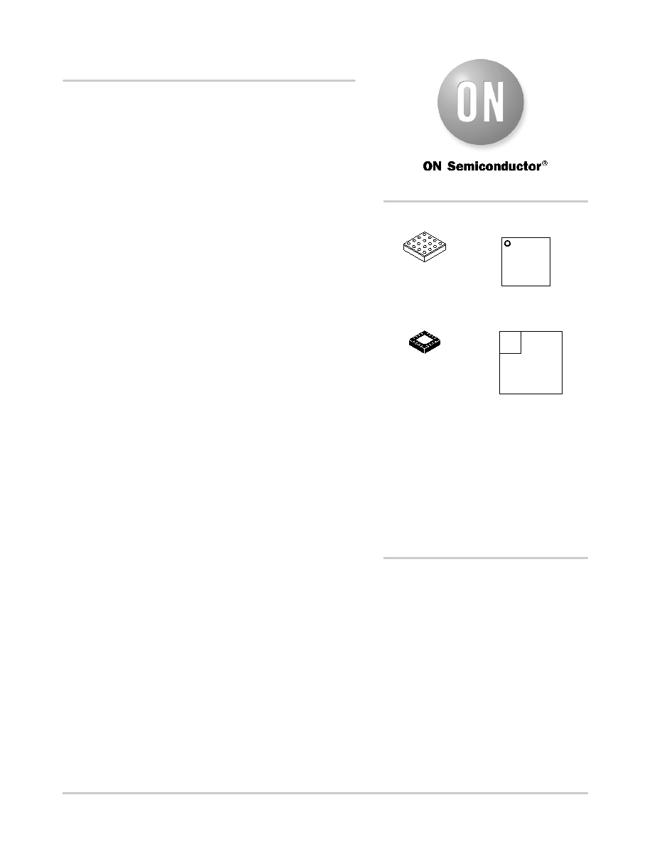
A
= Assembly Location
L
= Wafer Lot
Y
= Year
W
= Work Week
G
= PbFree Package
FCBGA16
BA SUFFIX
CASE 489
MARKING DIAGRAMS*
QFN16
MN SUFFIX
CASE 485G
http://onsemi.com
*For additional marking information, refer to
Application Note AND8002/D.
See detailed ordering and shipping information in the package
dimensions section on page 10 of this data sheet.
ORDERING INFORMATION
(Note: Microdot may be in either location)
SG
16
ALYWG
G
16
SG
16
ALYWG
G
1
相關(guān)PDF資料 |
PDF描述 |
|---|---|
| LFXP20C-4FN388I | IC FPGA 19.7KLUTS 388FPBGA |
| GBB90DHBS | CONN EDGECARD 180PS R/A .050 SLD |
| LFXP20C-5FN388C | IC FPGA 19.7KLUTS 388FPBGA |
| EMM44DRYI | CONN EDGECARD 88POS DIP .156 SLD |
| AYM31DRMT | CONN EDGECARD 62POS .156 WW |
相關(guān)代理商/技術(shù)參數(shù) |
參數(shù)描述 |
|---|---|
| NBSG16MNR2G | 功能描述:緩沖器和線路驅(qū)動(dòng)器 2.5V/3.3V SiGe Diff Receiver w/RSECL RoHS:否 制造商:Micrel 輸入線路數(shù)量:1 輸出線路數(shù)量:2 極性:Non-Inverting 電源電壓-最大:+/- 5.5 V 電源電壓-最小:+/- 2.37 V 最大工作溫度:+ 85 C 安裝風(fēng)格:SMD/SMT 封裝 / 箱體:MSOP-8 封裝:Reel |
| NBSG16VS | 制造商:ONSEMI 制造商全稱:ON Semiconductor 功能描述:2.5V/3.3V SiGe Differential Receiver/Driver with Variable Output Swing |
| NBSG16VS/D | 制造商:未知廠家 制造商全稱:未知廠家 功能描述:2.5V / 3.3V SiGe Differential Receiver/Driver with Variable Output Swing |
| NBSG16VSBA | 功能描述:緩沖器和線路驅(qū)動(dòng)器 2.5V/3.3V SiGe Diff RoHS:否 制造商:Micrel 輸入線路數(shù)量:1 輸出線路數(shù)量:2 極性:Non-Inverting 電源電壓-最大:+/- 5.5 V 電源電壓-最小:+/- 2.37 V 最大工作溫度:+ 85 C 安裝風(fēng)格:SMD/SMT 封裝 / 箱體:MSOP-8 封裝:Reel |
| NBSG16VSBAEVB | 功能描述:時(shí)鐘和定時(shí)器開發(fā)工具 BBG NBSG16VSBA EVAL BOARD RoHS:否 制造商:Texas Instruments 產(chǎn)品:Evaluation Modules 類型:Clock Conditioners 工具用于評估:LMK04100B 頻率:122.8 MHz 工作電源電壓:3.3 V |
發(fā)布緊急采購,3分鐘左右您將得到回復(fù)。