- 您現(xiàn)在的位置:買賣IC網(wǎng) > PDF目錄4577 > NBSG16MMNR2G (ON Semiconductor)IC RCVR/DRVR CML 2.5/3.3V 16-QFN PDF資料下載
參數(shù)資料
| 型號: | NBSG16MMNR2G |
| 廠商: | ON Semiconductor |
| 文件頁數(shù): | 10/11頁 |
| 文件大小: | 0K |
| 描述: | IC RCVR/DRVR CML 2.5/3.3V 16-QFN |
| 標準包裝: | 3,000 |
| 類型: | 收發(fā)器 |
| 應用: | 儀表 |
| 安裝類型: | 表面貼裝 |
| 封裝/外殼: | 16-VFQFN 裸露焊盤 |
| 供應商設備封裝: | 16-QFN(3x3) |
| 包裝: | 帶卷 (TR) |
NBSG16M
http://onsemi.com
8
Table 8. AC CHARACTERISTICS VCC = 0 V; VEE = 3.465 V to 2.375 V or VCC = 2.375 V to 3.465 V; VEE = 0 V
Symbol
Characteristic
40°C
25°C
85°C
Unit
Min
Typ
Max
Min
Typ
Max
Min
Typ
Max
VOUTPP Output Voltage Amplitude
fin < 7 GHz
fin < 10 GHz
300
200
400
250
300
200
400
250
300
100
400
150
mV
tPLH,
tPHL
Propagation Delay to
Output Differential
90
110
150
100
120
150
100
125
155
ps
tSKEW
Duty Cycle Skew (Note 16)
3
15
3
15
3
15
ps
tJITTER
RMS Random Clock Jitter (Note 18)
fin < 10 GHz
PeaktoPeak Data Dependent Jitter (Note 19)
fin < 10 Gb/s
0.2
8
1
15
0.2
8
1
15
0.2
8
1.0
15
ps
VINPP
Input Voltage Swing/Sensitivity
(Differential Configuration) (Note 17)
75
2500
75
2500
75
2500
mV
tr
tf
Output Rise/Fall Times @ 1 GHz
Q, Q
(20% 80%)
21
35
53
21
35
53
21
35
53
ps
NOTE: Device will meet the specifications after thermal equilibrium has been established when mounted in a test socket or printed circuit
board with maintained transverse airflow greater than 500 lfpm. Electrical parameters are guaranteed only over the declared
operating temperature range. Functional operation of the device exceeding these conditions is not implied. Device specification
limit values are applied individually under normal operating conditions and not valid simultaneously.
15.Measured using a 400 mV source, 50% duty cycle clock source. All loading with 50 W to VCC. Input edge rates 40 ps (20% 80%).
17.VINPP(max) cannot exceed VCC VEE. (Applicable only when VCC VEE < 2500 mV). Input voltage swing is a singleended measurement
operating in differential mode.
18.Additive RMS jitter with 50% duty cycle clock signal at 10GHz.
19.Additive PeaktoPeak data dependent jitter with NRZ PRBS2311 data rate at 10 Gb/s.
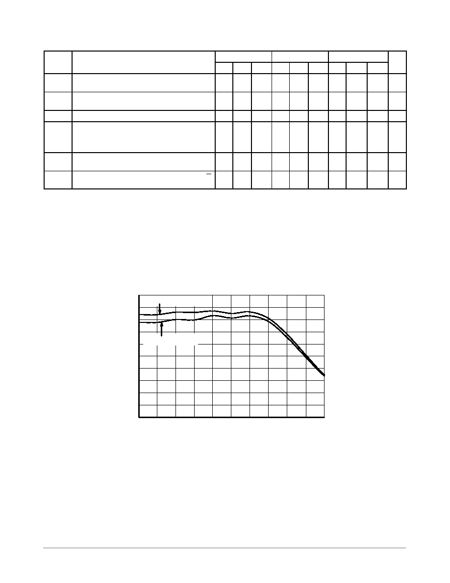
Figure 4. Output Voltage Amplitude (VOUTPP) versus
Input Clock Frequency (fin) at Ambient Temperature (Typical)
0
50
100
150
200
250
300
350
400
450
500
01
23456
789
10
FREQUENCY (GHz)
OUTPUT
VOL
TAGE
AMPLITUDE
(mV)
VCC VEE = 3.3 V
VCC VEE = 2.5 V
相關(guān)PDF資料 |
PDF描述 |
|---|---|
| ACC44DRXI | CONN EDGECARD 88POS .100 DIP SLD |
| NBSG16MNR2G | IC RCVR/DRVR RSECL SIGE DF 16QFN |
| ACB75DHLN | CONN EDGECARD 150PS .050 DIP SLD |
| ABB75DHLN | CONN EDGECARD 150PS .050 DIP SLD |
| HD9P6409-9Z | IC MED MANCHESTER 1MHZ 20-SOIC |
相關(guān)代理商/技術(shù)參數(shù) |
參數(shù)描述 |
|---|---|
| NBSG16MN | 功能描述:緩沖器和線路驅(qū)動器 2.5V/3.3V SiGe Diff RoHS:否 制造商:Micrel 輸入線路數(shù)量:1 輸出線路數(shù)量:2 極性:Non-Inverting 電源電壓-最大:+/- 5.5 V 電源電壓-最小:+/- 2.37 V 最大工作溫度:+ 85 C 安裝風格:SMD/SMT 封裝 / 箱體:MSOP-8 封裝:Reel |
| NBSG16MNG | 功能描述:緩沖器和線路驅(qū)動器 2.5V/3.3V SiGe Diff Receiver w/RSECL RoHS:否 制造商:Micrel 輸入線路數(shù)量:1 輸出線路數(shù)量:2 極性:Non-Inverting 電源電壓-最大:+/- 5.5 V 電源電壓-最小:+/- 2.37 V 最大工作溫度:+ 85 C 安裝風格:SMD/SMT 封裝 / 箱體:MSOP-8 封裝:Reel |
| NBSG16MNHTBG | 功能描述:緩沖器和線路驅(qū)動器 2.5/3.3V SIGE DF/RCV BBG RoHS:否 制造商:Micrel 輸入線路數(shù)量:1 輸出線路數(shù)量:2 極性:Non-Inverting 電源電壓-最大:+/- 5.5 V 電源電壓-最小:+/- 2.37 V 最大工作溫度:+ 85 C 安裝風格:SMD/SMT 封裝 / 箱體:MSOP-8 封裝:Reel |
| NBSG16MNR2 | 功能描述:緩沖器和線路驅(qū)動器 2.5V/3.3V SiGe Diff RoHS:否 制造商:Micrel 輸入線路數(shù)量:1 輸出線路數(shù)量:2 極性:Non-Inverting 電源電壓-最大:+/- 5.5 V 電源電壓-最小:+/- 2.37 V 最大工作溫度:+ 85 C 安裝風格:SMD/SMT 封裝 / 箱體:MSOP-8 封裝:Reel |
| NBSG16MNR2G | 功能描述:緩沖器和線路驅(qū)動器 2.5V/3.3V SiGe Diff Receiver w/RSECL RoHS:否 制造商:Micrel 輸入線路數(shù)量:1 輸出線路數(shù)量:2 極性:Non-Inverting 電源電壓-最大:+/- 5.5 V 電源電壓-最小:+/- 2.37 V 最大工作溫度:+ 85 C 安裝風格:SMD/SMT 封裝 / 箱體:MSOP-8 封裝:Reel |
發(fā)布緊急采購,3分鐘左右您將得到回復。