- 您現(xiàn)在的位置:買賣IC網(wǎng) > PDF目錄224596 > NAND01GR3A2AZA6 (STMICROELECTRONICS) 128M X 8 FLASH 1.8V PROM, 15000 ns, PBGA63 PDF資料下載
參數(shù)資料
| 型號: | NAND01GR3A2AZA6 |
| 廠商: | STMICROELECTRONICS |
| 元件分類: | PROM |
| 英文描述: | 128M X 8 FLASH 1.8V PROM, 15000 ns, PBGA63 |
| 封裝: | 8.50 X 15 MM, 1.20 MM HEIGHT, 0.80 MM PITCH, TFBGA-63 |
| 文件頁數(shù): | 16/56頁 |
| 文件大小: | 871K |
| 代理商: | NAND01GR3A2AZA6 |
第1頁第2頁第3頁第4頁第5頁第6頁第7頁第8頁第9頁第10頁第11頁第12頁第13頁第14頁第15頁當前第16頁第17頁第18頁第19頁第20頁第21頁第22頁第23頁第24頁第25頁第26頁第27頁第28頁第29頁第30頁第31頁第32頁第33頁第34頁第35頁第36頁第37頁第38頁第39頁第40頁第41頁第42頁第43頁第44頁第45頁第46頁第47頁第48頁第49頁第50頁第51頁第52頁第53頁第54頁第55頁第56頁
23/56
NAND128-A, NAND256-A, NAND512-A, NAND01G-A
Page Program
The Page Program operation is the standard oper-
ation to program data to the memory array.
The main area of the memory array is pro-
grammed by page, however partial page program-
ming is allowed where any number of bytes (1 to
528) or words (1 to 264) can be programmed.
The max number of consecutive partial page pro-
gram operations allowed in the same page is one
in the main area and two in the spare area. After
exceeding this a Block Erase command must be
issued before any further program operations can
take place in that page.
Before starting a Page Program operation a Point-
er operation can be performed to point to the area
to be programmed. Refer to the Pointer Opera-
tions section and Figure 12. for details.
Each Page Program operation consists of five
steps (see Figure 17.):
1.
one bus cycle is required to setup the Page
Program command
2.
four bus cycles are then required to input the
program address (refer to Table 6.)
3.
the data is then input (up to 528 Bytes/ 264
Words) and loaded into the Page Buffer
4.
one bus cycle is required to issue the confirm
command to start the P/E/R Controller.
5.
The P/E/R Controller then programs the data
into the array.
Once the program operation has started the Sta-
tus Register can be read using the Read Status
Register command. During program operations
the Status Register will only flag errors for bits set
to ’1’ that have not been successfully programmed
to ’0’.
During the program operation, only the Read Sta-
tus Register and Reset commands will be accept-
ed, all other commands will be ignored.
Once the program operation has completed the P/
E/R Controller bit SR6 is set to ‘1’ and the Ready/
Busy signal goes High.
The device remains in Read Status Register mode
until another valid command is written to the Com-
mand Interface.
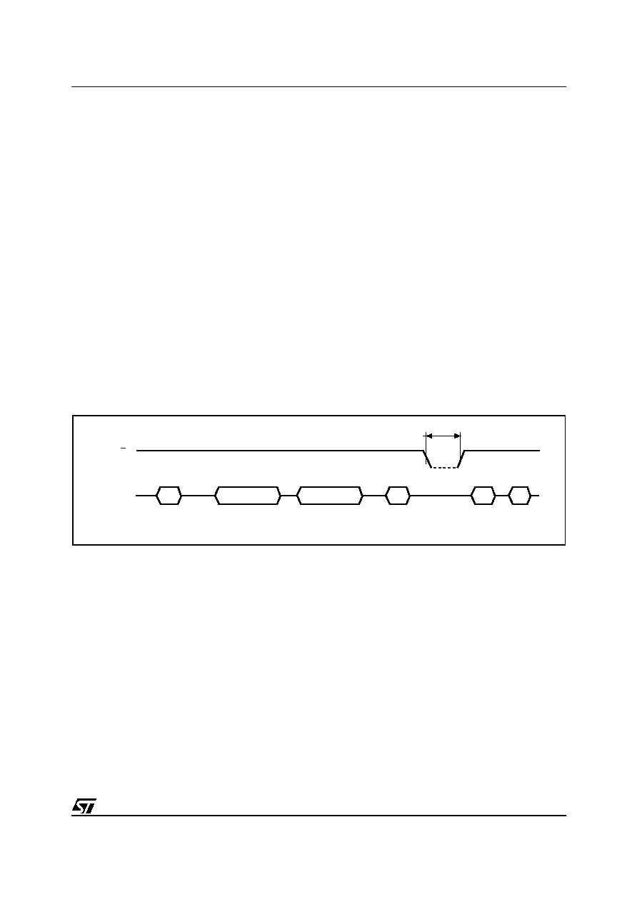
Figure 17. Page Program Operation
Note: Before starting a Page Program operation a Pointer operation can be performed. Refer to Pointer Operations section for details.
I/O
RB
Address Inputs
SR0
ai07566
Data Input
10h
70h
80h
Page Program
Setup Code
Confirm
Code
Read Status Register
Busy
tBLBH2
(Program Busy time)
相關PDF資料 |
PDF描述 |
|---|---|
| NAND01GR4B2BZA1F | 64M X 16 FLASH 1.8V PROM, 25000 ns, PBGA63 |
| NAND08GR4B3AZB6 | 512M X 16 FLASH 1.8V PROM, 25000 ns, PBGA63 |
| NAND256W4A2AZA6E | 16M X 16 FLASH 3V PROM, 12000 ns, PBGA55 |
| NCP303LSN41T1 | 1-CHANNEL POWER SUPPLY SUPPORT CKT, PDSO5 |
| NCS6416DWG | 8-CHANNEL, VIDEO MULTIPLEXER, PDSO20 |
相關代理商/技術參數(shù) |
參數(shù)描述 |
|---|---|
| NAND01GR3A2AZA6E | 制造商:STMICROELECTRONICS 制造商全稱:STMicroelectronics 功能描述:128 Mbit, 256 Mbit, 512 Mbit, 1 Gbit (x8/x16) 528 Byte/264 Word Page, 1.8V/3V, NAND Flash Memories |
| NAND01GR3A2AZA6F | 制造商:STMICROELECTRONICS 制造商全稱:STMicroelectronics 功能描述:128 Mbit, 256 Mbit, 512 Mbit, 1 Gbit (x8/x16) 528 Byte/264 Word Page, 1.8V/3V, NAND Flash Memories |
| NAND01GR3A2AZA6T | 制造商:STMICROELECTRONICS 制造商全稱:STMicroelectronics 功能描述:128 Mbit, 256 Mbit, 512 Mbit, 1 Gbit (x8/x16) 528 Byte/264 Word Page, 1.8V/3V, NAND Flash Memories |
| NAND01GR3A2AZB1 | 制造商:STMICROELECTRONICS 制造商全稱:STMicroelectronics 功能描述:128 Mbit, 256 Mbit, 512 Mbit, 1 Gbit (x8/x16) 528 Byte/264 Word Page, 1.8V/3V, NAND Flash Memories |
| NAND01GR3A2AZB1E | 制造商:STMICROELECTRONICS 制造商全稱:STMicroelectronics 功能描述:128 Mbit, 256 Mbit, 512 Mbit, 1 Gbit (x8/x16) 528 Byte/264 Word Page, 1.8V/3V, NAND Flash Memories |
發(fā)布緊急采購,3分鐘左右您將得到回復。