- 您現(xiàn)在的位置:買(mǎi)賣(mài)IC網(wǎng) > PDF目錄361068 > N16T1630C2BZ-70 (Electronic Theatre Controls, Inc.) 16Mb Ultra-Low Power Asynchronous CMOS SRAM PDF資料下載
參數(shù)資料
| 型號(hào): | N16T1630C2BZ-70 |
| 廠商: | Electronic Theatre Controls, Inc. |
| 英文描述: | 16Mb Ultra-Low Power Asynchronous CMOS SRAM |
| 中文描述: | 16Mb的超低功耗CMOS SRAM的異步 |
| 文件頁(yè)數(shù): | 2/9頁(yè) |
| 文件大?。?/td> | 245K |
| 代理商: | N16T1630C2BZ-70 |

The specifications of this device are subject to change without notice. For latest documentation see http://www.nanoamp.com.
(DOC#14-02-007 REV F ECN# 01-1103)
2
NanoAmp Solutions, Inc.
N16T1630C2B
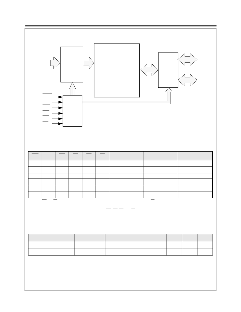
Functional Block Diagram
Functional Description
CE1
CE2
WE
OE
UB
LB
I/O
0
- I/O
151
1. When UB and LB are in select mode (low), I/O
0
- I/O
15
are affected as shown. When LB only is in the select mode only I/O
0
- I/O
7
are affected as shown. When UB is in the select mode only I/O
8
- I/O
15
are affected as shown.
2. When the device is in standby mode, control inputs (WE, OE, UB, and LB), address inputs and data input/outputs are internally
isolated from any external influence and disabled from exerting any influence externally.
3. When WE is invoked, the OE input is internally disabled and has no effect on the circuit.
MODE
POWER
H
X
X
X
X
X
High Z
Standby
2
Standby
2
Standby
Standby
X
L
X
X
X
X
High Z
Standby
L
H
X
X
X
3
H
L
1
L
1
L
1
H
L
1
L
1
L
1
High Z
Standby
L
H
L
Data In
Write
Active
L
H
H
L
Data Out
Read
Active
L
H
H
H
High Z
Active
Active
Capacitance
1
1. These parameters are verified in device characterization and are not 100% tested
Item
Symbol
Test Condition
Min
Max
Unit
Input Capacitance
C
IN
V
IN
= 0V, f = 1 MHz, T
A
= 25
o
C
V
IN
= 0V, f = 1 MHz, T
A
= 25
o
C
8
pF
I/O Capacitance
C
I/O
8
pF
Address
Inputs
A0 - A19
1M
x 16 bit
RAM Array
Input/
Output
Mux
and
Buffers
Address
Decode
Logic
Control
Logic
CE1
CE2
WE
OE
UB
LB
I/O0 - I/O7
I/O8 - I/O15
相關(guān)PDF資料 |
PDF描述 |
|---|---|
| N16T1630C2BZ2 | 16Mb Ultra-Low Power Asynchronous CMOS SRAM |
| N16T1630C2BZ2-55 | 16Mb Ultra-Low Power Asynchronous CMOS SRAM |
| N16T1630C2BZ2-70 | 16Mb Ultra-Low Power Asynchronous CMOS SRAM |
| N341256 | CMOS SRAM 256K-BIT(32KX8) |
| N341256P-12 | CMOS SRAM 256K-BIT(32KX8) |
相關(guān)代理商/技術(shù)參數(shù) |
參數(shù)描述 |
|---|---|
| N16T5620360 | 制造商:n/a 功能描述:_ |
| N16-T-56203-60 | 制造商:n/a 功能描述:_ |
| N16T75726 | 制造商:n/a 功能描述:_ |
| N16-T-75726 | 制造商:n/a 功能描述:_ |
| N17 | 制造商:Arcolectric 功能描述: |
發(fā)布緊急采購(gòu),3分鐘左右您將得到回復(fù)。