- 您現(xiàn)在的位置:買賣IC網 > PDF目錄361068 > N16T1630C2BZ2-55 (Electronic Theatre Controls, Inc.) 16Mb Ultra-Low Power Asynchronous CMOS SRAM PDF資料下載
參數(shù)資料
| 型號: | N16T1630C2BZ2-55 |
| 廠商: | Electronic Theatre Controls, Inc. |
| 英文描述: | 16Mb Ultra-Low Power Asynchronous CMOS SRAM |
| 中文描述: | 16Mb的超低功耗CMOS SRAM的異步 |
| 文件頁數(shù): | 1/9頁 |
| 文件大小: | 245K |
| 代理商: | N16T1630C2BZ2-55 |
NanoAmp Solutions, Inc.
1982 Zanker Road, San Jose, CA 95112
ph: 408-573-8878, FAX: 408-573-8877
www.nanoamp.com
N16T1630C2B
The specifications of this device are subject to change without notice. For latest documentation see http://www.nanoamp.com.
(DOC#14-02-007 REV F ECN# 01-1103)
1
16Mb Ultra-Low Power Asynchronous CMOS SRAM
1M x 16 bit
Overview
The N16T1630C2B is an integrated memory
device containing a low power 16 Mbit SRAM built
using a self-refresh DRAM array organized as
1,024,576 words by 16 bits. It is designed to be
identical in operation and interface to standard 6T
SRAMS. The device is designed for low standby
and operating current and includes a power-down
feature to automatically enter standby mode. The
device operates with two chip enable (CE1 and
CE2) controls and output enable (OE) to allow for
easy memory expansion. Byte controls (UB and
LB) allow the upper and lower bytes to be
accessed independently and can also be used to
deselect the device. The N16T1630C2B is optimal
for various applications where low-power is critical
such as battery backup and hand-held devices.
The device can operate over a very wide
temperature range of -40
o
C to +85
o
C and is
available in JEDEC standard BGA packages
compatible with other standard 1Mb x 16 SRAMs.
Features
Single Wide Power Supply Range
2.7 to 3.6 Volts
Very low standby current
100μA at 3.0V (Max)
Very low operating current
2.0mA at 3.0V and 1μs (Typical)
Simple memory control
Dual Chip Enables (CE1 and CE2)
Byte control for independent byte operation
Output Enable (OE) for memory expansion
Very fast access time
55ns address access option
35ns OE access time
Automatic power down to standby mode
TTL compatible three-state output driver
Green option for BGA package
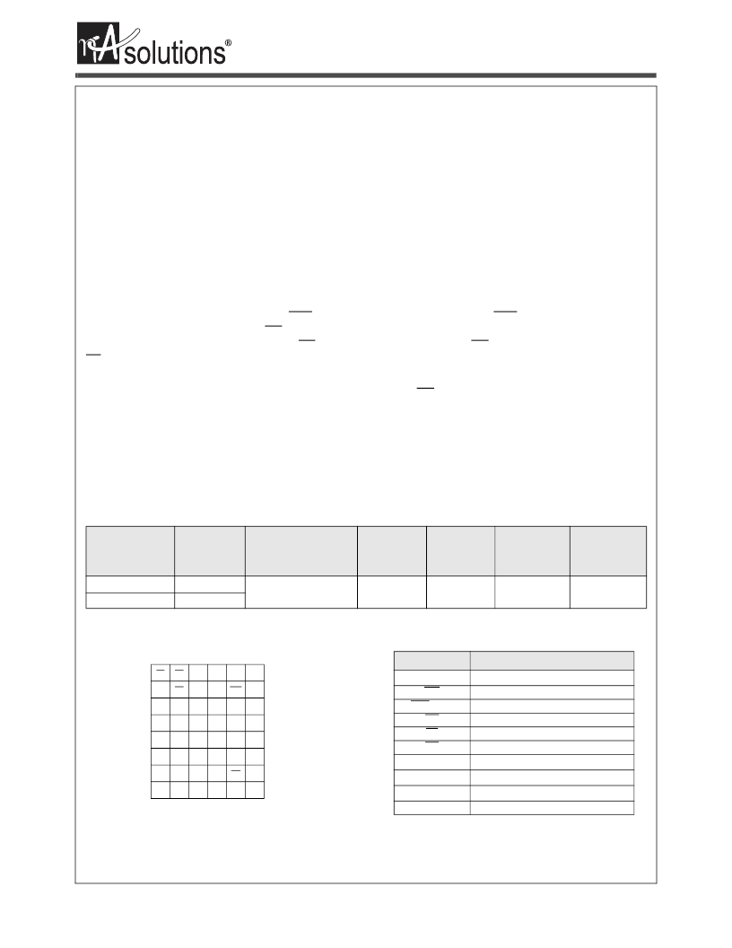
Pin Configuration (Top View)
Pin Description
Product Family
Part Number
Package
Type
Operating
Temperature
Power
Supply (Vcc)
Speed
Standby
Current (I
SB
),
Max @ 3.0V
Operating
Current (Icc),
Max
N16T1630C2BZ
48 - BGA
-40
o
C to +85
o
C
2.7V - 3.6V
70ns
55ns
100
μ
A
3 mA @ 1MHz
N16T1630C2BZ2 Green 48 - BGA
1
2
3
4
5
6
A
LB
OE
A
0
A
1
A
2
CE2
B
I/O
8
UB
A
3
A
4
CE1
I/O
0
C
I/O
9
I/O
10
A
5
A
6
I/O
1
I/O
2
D
V
SS
I/O
11
A
17
A
7
I/O
3
V
CC
E
V
CC
I/O
12
NC
A
16
I/O
4
V
SS
F
I/O
14
I/O
13
A
14
A
15
I/O
5
I/O
6
G
I/O
15
A
19
A
12
A
13
WE
I/O
7
H
A
18
A
8
A
9
A
10
A
11
NC
48 Ball BGA
6 x 8 mm
Pin Name
Pin Function
A
0
-A
19
WE
CE1, CE2
OE
LB
UB
I/O
0
-I/O
15
V
CC
V
SS
NC
Address Inputs
Write Enable Input
Chip Enable Input
Output Enable Input
Lower Byte Enable Input
Upper Byte Enable Input
Data Inputs/Outputs
Power
Ground
Not Connected
相關PDF資料 |
PDF描述 |
|---|---|
| N16T1630C2BZ2-70 | 16Mb Ultra-Low Power Asynchronous CMOS SRAM |
| N341256 | CMOS SRAM 256K-BIT(32KX8) |
| N341256P-12 | CMOS SRAM 256K-BIT(32KX8) |
| N341256P-15 | CMOS SRAM 256K-BIT(32KX8) |
| N341256P-20 | CMOS SRAM 256K-BIT(32KX8) |
相關代理商/技術參數(shù) |
參數(shù)描述 |
|---|---|
| N16T1630C2BZ2-70 | 制造商:未知廠家 制造商全稱:未知廠家 功能描述:16Mb Ultra-Low Power Asynchronous CMOS SRAM |
| N16T1630C2BZ-55 | 制造商:未知廠家 制造商全稱:未知廠家 功能描述:16Mb Ultra-Low Power Asynchronous CMOS SRAM |
| N16T1630C2BZ-70 | 制造商:NANOAMP 制造商全稱:NANOAMP 功能描述:16Mb Ultra-Low Power Asynchronous CMOS SRAM |
| N16T5620360 | 制造商:n/a 功能描述:_ |
| N16-T-56203-60 | 制造商:n/a 功能描述:_ |
發(fā)布緊急采購,3分鐘左右您將得到回復。