- 您現(xiàn)在的位置:買賣IC網(wǎng) > PDF目錄383645 > MT9162 (Mitel Networks Corporation) ISO2-CMOS 5 Volt Single Rail Codec PDF資料下載
參數(shù)資料
| 型號: | MT9162 |
| 廠商: | Mitel Networks Corporation |
| 元件分類: | Codec |
| 英文描述: | ISO2-CMOS 5 Volt Single Rail Codec |
| 中文描述: | ISO2 - 5伏的CMOS單鐵編解碼器 |
| 文件頁數(shù): | 2/17頁 |
| 文件大?。?/td> | 83K |
| 代理商: | MT9162 |
MT9162
Advance Information
7-162
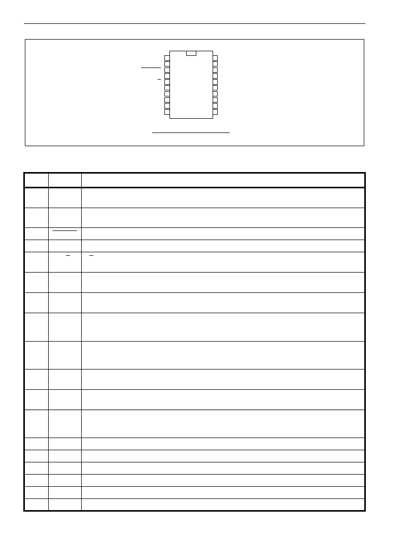
Figure 2 - Pin Connections
Pin Description
Pin #
Name
Description
1
V
Bias
Bias Voltage (Output).
(V
DD
/2) volts is available at this pin for biasing external amplifiers.
Connect 0.1
μ
F capacitor to V
SS
. Connect 1
μ
F capacitor to Vref.
Reference Voltage for Codec (Output).
Nominally [(V
DD
/2)-1.9] volts. Used internally.
Connect 0.1
μ
F capacitor to V
SS
. Connect 1
μ
F capacitor to VBias
PWRST
Power-up Reset.
Resets internal state of device via Schmitt Trigger input (active low).
2
V
Ref
3
4
IC
Internal Connection.
Tie externally to V
SS
for normal operation.
A/
μ
Law Selection
. CMOS level compatable input pin governs the companding law used by
the device. A-law selected when pin tied to V
DD
or
μ
-law selected when pin tied to V
SS
.
RXMute
Receive Mute.
When 1, the transmit PCM is forced to negative zero code. When 0, normal
operation. CMOS level compatible.
5
A/
μ
6
7
TXMute
Transmit Mute.
When 1, the transmit PCM is forced to negative zero code. When 0, normal
operation. CMOS level compatible.
8
9
10
CSL0
CSL1
CSL2
Clock Speed Select.
These pins are used to program the speed of the SSI mode as well as
the conversion rate between the externally supplied MCL clock and the 512 kHz clock required
by the filter/codec. Refer to Table 2 for details. CMOS level compatible.
11
D
out
Data Output.
A tri-state digital output for 8-bit wide channel data being sent to the Layer 1
device. Data is shifted out via the pin concurrent with the rising edge of BCL during the timeslot
defined by STB.
12
D
in
Data Input.
A digital input for 8-bit wide data from the layer 1 device. Data is sampled on the
falling edge of BCL during the timeslot defined by STB. CMOS level compatible.
13
STB
Data Strobe.
This input determines the 8-bit timeslot used by the device for both transmit and
receive data. This active high signal has a repetition rate of 8 kHz. CMOS level compatible.
14
CLOCKin
Clock (Input).
The clock provided to this input pin is used by the internal device functions.
Connect bit clock to this pin when it is 512 kHz or greater. Connect a 4096 kHz clock to this pin
when the bit clock is 128 kHz or 256 kHz. CMOS level compatible.
15
V
DD
AOUT-
Positive Power Supply.
Nominally 5 volts.
16
Inverting Analog Output.
(balanced).
17
AOUT+
Non-Inverting Analog Output.
(balanced).
18
V
SS
Ain-
Ground.
Nominally 0 volts.
19
Inverting Analog Input.
No external anti-aliasing is required.
20
Ain+
Non-Inverting Analog Input.
Non-inverting input. No external anti-aliasing is required.
AIN-
VSS
AOUT +
AOUT -
VDD
CLOCKin
AIN+
VBias
VRef
PWRST
IC
RXMUTE
TXMUTE
CSL0
CSL1
CSL2
Din
Dout
1
2
3
4
5
6
7
8
9
10
11
12
13
14
15
16
20
19
18
17
STB
20 PIN PDIP/SOIC/SSOP
A/
μ
相關(guān)PDF資料 |
PDF描述 |
|---|---|
| MT9171 | Digital Subscriber Interface Circuit with RxSB(數(shù)字用戶接口電路(帶接收同步位)) |
| MT9172 | Digital Network Interface Circuit with RxSB(數(shù)字網(wǎng)絡(luò)接口電路(帶接收同步位)) |
| MT9173AE | Digital Subscriber Interface Circuit with RxSB |
| MT9173AN | Digital Subscriber Interface Circuit with RxSB |
| MT9173AP | Digital Subscriber Interface Circuit with RxSB |
相關(guān)代理商/技術(shù)參數(shù) |
參數(shù)描述 |
|---|---|
| MT9162AE | 制造商:Microsemi Corporation 功能描述:CODEC 20PDIP - Rail/Tube |
| MT9162AN | 制造商:ZARLINK 制造商全稱:Zarlink Semiconductor Inc 功能描述:5 Volt Single Rail Codec |
| MT9162AN1 | 制造商:Microsemi Corporation 功能描述:CODEC A/ULAW 5V SSOP 制造商:Microsemi Corporation 功能描述:CODEC 20SSOP - Rail/Tube 制造商:MICROSEMI CONSUMER MEDICAL PRODUCT GROUP 功能描述:IC CODEC MFC 5V 20SSOP |
| MT9162AS | 制造商:Microsemi Corporation 功能描述:CODEC 20SOIC W - Rail/Tube 制造商:MICROSEMI CONSUMER MEDICAL PRODUCT GROUP 功能描述:IC CODEC MFC 5V 20SOIC 制造商:Microsemi Corporation 功能描述:IC CODEC MFC 5V 20SOIC |
| MT9171 | 制造商:ZARLINK 制造商全稱:Zarlink Semiconductor Inc 功能描述:ISO2-CMOS ST-BUS FAMILY |
發(fā)布緊急采購,3分鐘左右您將得到回復(fù)。