- 您現(xiàn)在的位置:買賣IC網(wǎng) > PDF目錄383643 > MT8950 (Mitel Networks Corporation) ISO-CMOS ST-BUS⑩ FAMILY Data Codec PDF資料下載
參數(shù)資料
| 型號(hào): | MT8950 |
| 廠商: | Mitel Networks Corporation |
| 元件分類: | Codec |
| 英文描述: | ISO-CMOS ST-BUS⑩ FAMILY Data Codec |
| 中文描述: | 異意法半導(dǎo)體的CMOS總線⑩系列數(shù)據(jù)編解碼器 |
| 文件頁(yè)數(shù): | 2/16頁(yè) |
| 文件大小: | 223K |
| 代理商: | MT8950 |
第1頁(yè)當(dāng)前第2頁(yè)第3頁(yè)第4頁(yè)第5頁(yè)第6頁(yè)第7頁(yè)第8頁(yè)第9頁(yè)第10頁(yè)第11頁(yè)第12頁(yè)第13頁(yè)第14頁(yè)第15頁(yè)第16頁(yè)
MT8950
ISO-CMOS
6-4
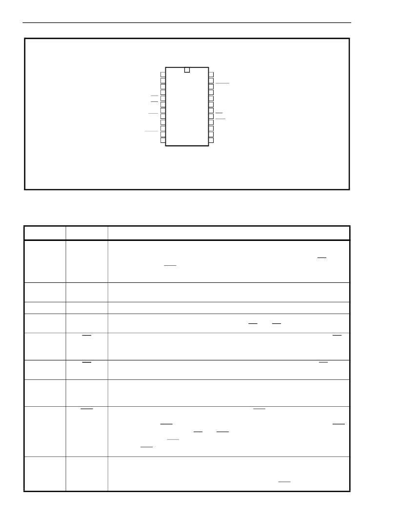
Figure 2 - Pin Connections
Pin Description
Pin #
Name
Description
1
CSTi
Control ST-BUS In (TTL Input) -
This ST-BUS interface pin accepts a serial input
stream which loads the Control Register. The mode of operation of the
device, the bits in the Violation word, and, the resetting of Data Activity (DA) and
Scan Point output (SPo) are controlled by this register. The contents of the register
are updated once every ST-BUS frame when the interface is enabled.
2
DSTi
Data ST-BUS In (TTL Input) -
Accepts the 8 bits of TEM Data when the ST-BUS
interface is enabled.
3
C2i
2.048 MHz Clock (TTL Input) -
This is the input for the 2.048 MHz clock.
4
DSTo
ST-BUS Output (Three-State Output) -
This is the 2.048 Mbps serial output for
theTEM encoded word. It is enabled when both F1i and CA are low.
5
F1i
Framing Type 1 Input (TTL Input) -
This active low input, in conjunction with CA,
enables the ST-BUS interface (DSTi, DSTo and CSTi). It is internally sampled on
every positive edge of the C2i clock and provides frame synchronization.
CA
Control Address (TTL Input) -
This active low input (in conjunction with F1i)
enables the ST-BUS interface.
7
DF
Data Format Select (CMOS Input) -
When HIGH, the Data Codec accepts and
delivers the data in unipolar Return to Zero (RZ) format. When LOW, the data
format is unipolar NRZ.
8
RxE
Received Energy Signal (Schmitt Input) -
When RxE goes LOW it establishes the
polarity of the input pins D
X
1 and D
X
2 in the RZ mode. The input which received the
last pulse before RxE goes LOW is established as the unipolar MARK input. RxE
also enables the operation of DA and SPo outputs the loopback modes (Modes 4, 5
and 6) of the codec, RxE is forced to the LOW state internally independent of the pin
condition. RxE should be exerted LOW for the duration of a data call.
9
D
X
1
Data Transmit 1 (Schmitt Input) -
If DF= LOW, accepts data in the NRZ format.
(HIGH = MARK, LOW = SPACE).
If DF=HIGH, accepts active low unipolar pulses representing the digital data in the
RZ format. MARK or SPACE polarity is established by the RxE input.
1
2
3
4
5
6
7
8
9
10
11
12
13
14
15
16
24
23
22
21
20
19
18
17
CSTi
DSTi
C2i
DSTo
F1i
CA
DF
RxE
DX1
DX2
NRZo
VSS
VDD
NC
PRST
NC
NC
DR1
DR2
DA
SPo
SPi
DP
SCLK
相關(guān)PDF資料 |
PDF描述 |
|---|---|
| MT8950AC | ISO-CMOS ST-BUS⑩ FAMILY Data Codec |
| MT8952BC | ISO-CMOS ST-BUS⑩ FAMILY HDLC Protocol Controller |
| MT8952BE | ISO-CMOS ST-BUS⑩ FAMILY HDLC Protocol Controller |
| MT8952BP | ISO-CMOS ST-BUS⑩ FAMILY HDLC Protocol Controller |
| MT8952BS | ISO-CMOS ST-BUS⑩ FAMILY HDLC Protocol Controller |
相關(guān)代理商/技術(shù)參數(shù) |
參數(shù)描述 |
|---|---|
| MT8950AC | 制造商:MITEL 制造商全稱:Mitel Networks Corporation 功能描述:ISO-CMOS ST-BUS⑩ FAMILY Data Codec |
| MT8952 | 制造商:MITEL 制造商全稱:Mitel Networks Corporation 功能描述:ISO-CMOS ST-BUS⑩ FAMILY HDLC Protocol Controller |
| MT8952B | 制造商:MITEL 制造商全稱:Mitel Networks Corporation 功能描述:ISO-CMOS ST-BUS⑩ FAMILY HDLC Protocol Controller |
| MT8952B-1 | 制造商:MITEL 制造商全稱:Mitel Networks Corporation 功能描述:ISO-CMOS ST-BUS⑩ FAMILY HDLC Protocol Controller |
| MT8952BC | 制造商:MITEL 制造商全稱:Mitel Networks Corporation 功能描述:ISO-CMOS ST-BUS⑩ FAMILY HDLC Protocol Controller |
發(fā)布緊急采購(gòu),3分鐘左右您將得到回復(fù)。