- 您現在的位置:買賣IC網 > PDF目錄383641 > MT884 (Mitel Networks Corporation) () PDF資料下載
參數資料
| 型號: | MT884 |
| 廠商: | Mitel Networks Corporation |
| 英文描述: | () |
| 中文描述: | () |
| 文件頁數: | 5/11頁 |
| 文件大小: | 87K |
| 代理商: | MT884 |
Application Note
MSAN-144
A-233
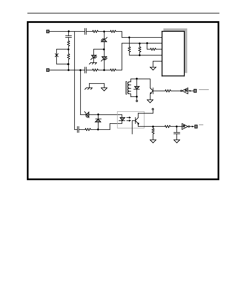
Figure 2 - Line Interface with Protection, Termination and Ring Detector
this function as shown in Fig. 2. When relay K1 is
activated (during data reception), the telephone line
is terminated with 600
(R1) and 2.2
μ
F (C1). A
430k resistor (R2) ensures that capacitor C1 is
biased with the 48V CO (central office) battery
voltage when relay K1 is not activated. This reduces
undesirable transients when the termination circuit is
activated.
TIP
RING
K1
C1
R1
R2
C2
R3
R5
R4
R6
D5
D4
D6
C3
Earth
Ground
Internal
Ground
R7
IN+
IN-
GS
VRef
VSS
K1
D1
Q1
R10
R8
R9
MT8841
RELAY
RD
U2B
VDD
VDD
D3
U1
R11
C4
D2
R12
R13
C5
Components List:
U1
U2
D2, D1
D3, D4, D5, D6
Q1
C2, C3
C5
C4
C1
R10
4N25, Opto-Coupler
74HC14, Inverter Schitt Hex
IN4004, 400V 1A, Rectifier General
IN5245B, 15V 1/2W, Zener General
2N3904, 40V 200mA, Transistor NPN
0.022
μ
, 400V 5%, Capacitor Polyester
0.33
μ
, 50V 20%, Capacitor Ceramic
0.33
μ
, 250V 5%, Capacitor Polyester
2
μ
2, 250V 5%, Capacitor Polyester
1k, 1/2W 1%, Resistor Metal
R5, R6
R7
R8
R13
R12
R9
R1
R11
R2, R3, R4
K1
34K, 1/2W 1%, Resistor Metal
53k6, 1/2W 1%, Resistor Metal
60k4, 1/2W 1%, Resistor Metal
140k, 1/2W 1%, Resistor Metal
301k, 1/2W 1%, Resistor Metal
464k, 1/2W 1%, Resistor Metal
600r, 1/2W 5%, Resistor Fusible
12k, 1W5 5%, Resistor Fusible
430k, 3W 5%, Resistor Power 1KV
RDPDT, 5V 28mA, Relay DPDT
U2A
The high impedance isolation circuit protects the
user and the low voltage circuitry from high voltage
fault conditions which may occur on the line. The
high power resistors and high voltage capacitors
(C2, C3, R3, R4), were selected to meet most line
fault conditions. The high impedance components
limit the current, while the zener's (D4, D5, D6) limit
the voltage. Relay K1 and opto-coupler U1 also
provide physical isolation.
In the ringing detector of Figure 2, the ringing
response is determined mainly by the charge time of
C5 through R13, as well as the positive going
threshold of the CMOS Schmitt trigger. The ringing
detector decay time is determined mainly by the
discharge time of C5 through R12 and R13, as well
as the negative going threshold of the CMOS
Schmitt trigger. Typical response time is 150ms and
typical decay time is also 150ms.
The FSK signal data is input to the MT8841 through
a differential amplifier configuration with overall gain
of unity. To increase the common mode rejection
range, a modified differential input configuration is
used. A voltage divider of R7 (53.6k) and R3 + R5
(464k) reduces the op-amp signal at the positive
input by 9.66 times. To maintain an overall gain of 1,
the attenuation due to the voltage divider must be
cancelled. This is achieved by increasing the op-
amp gain to 9.66. Therefore, 9.66 = 1 + R9/(R8//
(R4+R6)); with R9 at 464k, R8 is 60.4k. Since the
op-amp common mode range is 3Vpp, the maximum
common mode input signal that this circuit can
cancel is 3Vpp 9.66 = 29Vpp = 10.2Vrms.
相關PDF資料 |
PDF描述 |
|---|---|
| MT8860 | DTMF DECODER |
| MT8860XC | DTMF DECODER |
| MT8860XE | DTMF DECODER |
| MT8865 | DTMF Filter |
| MT8865XC | DTMF Filter |
相關代理商/技術參數 |
參數描述 |
|---|---|
| MT8840 | 制造商:MITEL 制造商全稱:Mitel Networks Corporation 功能描述:ISO2-CMOS Data Over Voice Modem |
| MT8840-1 | 制造商:MITEL 制造商全稱:Mitel Networks Corporation 功能描述:ISO2-CMOS Data Over Voice Modem |
| MT8840AE | 制造商:Rochester Electronics LLC 功能描述: 制造商:MITEL / ZARLINK 功能描述: 制造商:Zarlink Semiconductor Inc 功能描述: |
| MT8840AS | 制造商:MITEL 制造商全稱:Mitel Networks Corporation 功能描述:ISO2-CMOS Data Over Voice Modem |
| MT8841 | 制造商:MITEL 制造商全稱:Mitel Networks Corporation 功能描述:CMOS Calling Number Identification Circuit |
發(fā)布緊急采購,3分鐘左右您將得到回復。