- 您現(xiàn)在的位置:買賣IC網(wǎng) > PDF目錄384755 > MT48LC32M16A2 (Micron Technology, Inc.) SYNCHRONOUS DRAM PDF資料下載
參數(shù)資料
| 型號: | MT48LC32M16A2 |
| 廠商: | Micron Technology, Inc. |
| 英文描述: | SYNCHRONOUS DRAM |
| 中文描述: | 同步DRAM |
| 文件頁數(shù): | 22/55頁 |
| 文件大小: | 1828K |
| 代理商: | MT48LC32M16A2 |
第1頁第2頁第3頁第4頁第5頁第6頁第7頁第8頁第9頁第10頁第11頁第12頁第13頁第14頁第15頁第16頁第17頁第18頁第19頁第20頁第21頁當前第22頁第23頁第24頁第25頁第26頁第27頁第28頁第29頁第30頁第31頁第32頁第33頁第34頁第35頁第36頁第37頁第38頁第39頁第40頁第41頁第42頁第43頁第44頁第45頁第46頁第47頁第48頁第49頁第50頁第51頁第52頁第53頁第54頁第55頁
22
512Mb: x4, x8, x16 SDRAM
512MSDRAM_D.p65
–
Rev. D; Pub 1/02
Micron Technology, Inc., reserves the right to change products or specifications without notice.
2000, Micron Technology, Inc.
512Mb: x4, x8, x16
SDRAM
ADVANCE
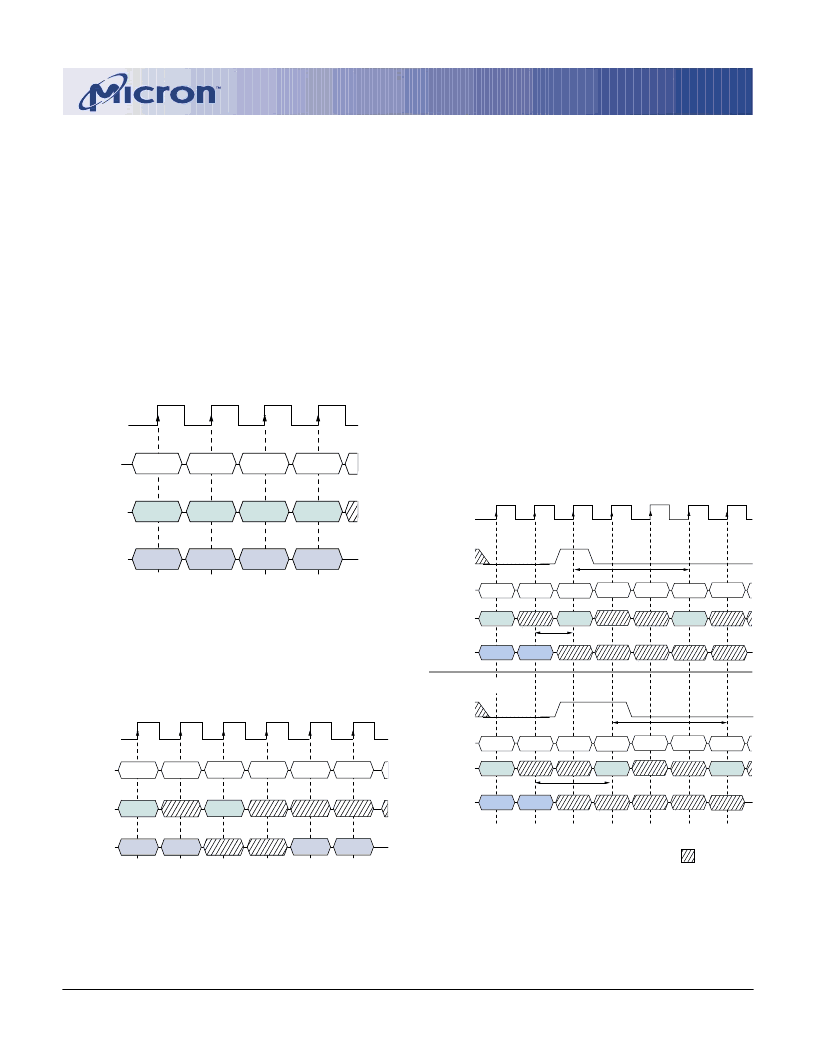
registered. The auto precharge mode requires a
t
WR of at
least one clock plus time, regardless of frequency. In
addition, when truncating a WRITE burst, the DQM sig-
nal must be used to mask input data for the clock edge
prior to, and the clock edge coincident with, the
PRECHARGE command. An example is shown in Figure
18. Data
n
+ 1 is either the last of a burst of two or the last
desired of a longer burst. Following the PRECHARGE
command, a subsequent command to the same bank
cannot be issued until
t
RP is met. The precharge can be
issued coincident with the first coincident clock edge (T2
in Figure 18) on an A1 Version and with the second clock
on an A2 Version (Figure 18.)
In the case of a fixed-length burst being executed to
completion, a PRECHARGE command issued at the opti-
mum time (as described above) provides the same op-
eration that would result from the same fixed-length
burst with auto precharge. The disadvantage of the
PRECHARGE command is that it requires that the com-
mand and address buses be available at the appropriate
time to issue the command; the advantage of the
Figure 18
WRITE To PRECHARGE
DON
’
T CARE
DQM
CLK
DQ
T2
T1
T4
T3
T0
COMMAND
ADDRESS
BANK
a
,
COL
n
T5
NOP
WRITE
PRECHARGE
NOP
NOP
D
IN
n
D
IN
n
+ 1
ACTIVE
tRP
BANK
(
a
or all)
t
WR
BANK
a
,
ROW
DQM
DQ
COMMAND
ADDRESS
COL
a
,
n
NOP
WRITE
PRECHARGE
NOP
NOP
D
IN
n
D
IN
n
+ 1
ACTIVE
tRP
BANK
(
a
or all)
t
WR
NOTE:
DQM could remain LOW in this example if the WRITE burst is a fixed length of two.
BROW
a
,
T6
NOP
NOP
tWR @ tCLK
≥
15ns
tWR = tCLK < 15ns
Data for any WRITE burst may be truncated with a
subsequent READ command, and data for a fixed-length
WRITE burst may be immediately followed by a READ
command. Once the READ command is registered, the
data inputs will be ignored, and WRITEs will not be
executed. An example is shown in Figure 17. Data
n
+ 1 is
either the last of a burst of two or the last desired of a
longer burst.
Data for a fixed-length WRITE burst may be followed
by, or truncated with, a PRECHARGE command to the
same bank (provided that auto precharge was not acti-
vated), and a full-page WRITE burst may be truncated
with a PRECHARGE command to the same bank. The
PRECHARGE command should be issued
t
WR after the
clock edge at which the last desired input data element is
Figure 17
WRITE To READ
CLK
DQ
T2
T1
T3
T0
COMMAND
ADDRESS
NOP
WRITE
BANK,
COL
n
D
IN
n
D
IN
n
+ 1
D
OUT
b
READ
NOP
NOP
BANK,
COL
b
NOP
D
OUT
b
+ 1
T4
T5
NOTE:
The WRITE command may be to any bank, and the READ command
may be to any bank. DQM is LOW. CAS latency = 2 for illustration.
Figure 16
Random WRITE Cycles
CLK
DQ
D
IN
n
T2
T1
T3
T0
COMMAND
ADDRESS
WRITE
BANK,
COL
n
D
IN
a
D
IN
x
D
IN
m
WRITE
WRITE
WRITE
BANK,
COL
a
BANK,
COL
x
BANK,
COL
m
NOTE:
Each WRITE command may be to any bank.
DQM is LOW.
相關PDF資料 |
PDF描述 |
|---|---|
| MT48LC8M16A2FB-75LIT | SYNCHRONOUS DRAM |
| MT48LC8M16A2FB-7E | SYNCHRONOUS DRAM |
| MT48LC8M16A2FB-7EIT | SYNCHRONOUS DRAM |
| MT48LC8M16A2FB-7EL | SYNCHRONOUS DRAM |
| MT48LC8M16A2FB-7ELIT | SYNCHRONOUS DRAM |
相關代理商/技術參數(shù) |
參數(shù)描述 |
|---|---|
| MT48LC32M16A2-75ITC | 制造商:Micron Technology Inc 功能描述: |
| MT48LC32M16A2P-75 | 制造商:Micron Technology Inc 功能描述: |
| MT48LC32M16A2P-75 C TR | 制造商:Micron Technology Inc 功能描述:DRAM Chip SDRAM 512M-Bit 32Mx16 3.3V 54-Pin TSOP-II T/R 制造商:Micron Technology 功能描述:DRAM Chip SDRAM 512M-Bit 32Mx16 3.3V 54-Pin TSOP-II T/R |
發(fā)布緊急采購,3分鐘左右您將得到回復。