- 您現(xiàn)在的位置:買賣IC網(wǎng) > PDF目錄358227 > MSK5827HRHUA (MS KENNEDY CORP) ADJUSTABLE POSITIVE LDO REGULATOR, CSFM5 PDF資料下載
參數(shù)資料
| 型號(hào): | MSK5827HRHUA |
| 廠商: | MS KENNEDY CORP |
| 元件分類: | 可調(diào)正電壓單路輸出LDO穩(wěn)壓器 |
| 英文描述: | ADJUSTABLE POSITIVE LDO REGULATOR, CSFM5 |
| 封裝: | HERMETIC SEALED, SIP-5 |
| 文件頁數(shù): | 3/6頁 |
| 文件大?。?/td> | 193K |
| 代理商: | MSK5827HRHUA |
APPLICATION NOTES
PIN FUNCTIONS
VIN -
This pin provides power to all internal circuitry in-
cluding bias, start-up, thermal limit and overcurrent latch.
Input voltage range is 2.9V to 6.5V.
GND -
Internally connected to ground, this pin should be
connected externally by the user to the circuit ground.
SHUTDOWN -
There are two functions to the SHUTDOWN
pin. It may be used to disable the output voltage or to
reset a current latch condition. To activate the shutdown/
reset functions the user must apply a voltage greater than
1.6V to the SHUTDOWN pin. The output voltage will turn
on when the SHUTDOWN pin is pulled below the thresh-
old voltage. If the SHUTDOWN pin is not used, it should
be connected to ground. It should be noted that with the
shutdown pin tied to ground, a current latch condition
can only be reset by cycling power off, then on.
VOUT -
This is the output pin for the device.
ADJ UST -
The ADJ UST pin is the inverting input of the
internal error amplifier. The non-inverting input is con-
nected to an internal 1.265V reference. This error ampli-
fier controls the drive to the output transistor to force the
ADJ UST pin to 1.265V. An external resistor divider is
connected to the output, ADJ UST pin and ground to set
the output voltage.
OUTPUT CAPACITOR SELECTION
Output capacitors are required to maintain regulation
and stability. Two 4.7μF and three 470μF surface mount
tantalum capacitor from the output to ground should suf-
fice under most conditions. Ceramic output capacitors
(0.1μF typical) should be placed directly across the load
power connections as close to the load as possible. If the
user finds that tighter voltage regulation is needed during
output transients, more capacitance may be added. If more
capacitance is added to the output, the bandwidth may
suffer.
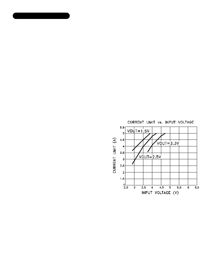
CURRENT LIMIT AND SOA
The MSK 5827RH current limit function is directly af-
fected by the input and output voltages. Figure 1 illus-
trates the relationship between VIN and ICL for various
output voltages. It is very important for the user to con-
sult the SOA curve when using input voltages which re-
sult in current limit conditions beyond 4.5 Amps. When
using input voltages which result in current limit above
4.5 Amps, the user must maintain output current within
the SOA curve to avoid damage to the device. Note that 5
Amp maximum is due to current carrying capability of the
internal wirebonds.
3
OVERCURRENT LATCH
Overcurrent protection is provided by the MSK 5827RH
series through the use of a timed latch off circuit. The
internal latch timeout is triggered by an overcurrent con-
dition. To allow for start up surge currents, the timeout is
approximately 5.5mS at 25° C. If the overcurrent condi-
tion remains at the end of the timeout cycle, the regulator
will latch off until the latch is reset. Reset the latch by
pulling the shutdown pin high or cycling VIN off then back
on. A thermal limit condition will trigger the latch with no
time out delay. The adjust pin is also used for external
compensation. See compensating the MSK 5827RH for
additonal information.
INPUT POWER SUPPLY BYPASSING
To maximize transient response and minimize power
supply transients it is recommended that a 100μF tanta-
lum capacitor is connected between VIN and ground. A
0.1μF ceramic capacitor should also be used for high fre-
quency bypassing.
FIGURE 1
Rev. B 1/10
COMPENSATING THE MSK 5827RH
The MSK 5827RH is externally compensated for opti-
mal stability. An RC network around the feedback divider
can be tailored to a variety of applications. The values
shown in the typical application circuit provide a starting
point when combined with the recomended output ca-
pacitance.
相關(guān)PDF資料 |
PDF描述 |
|---|---|
| MSM-2170-FX-BMA-02 | 0 MHz - 18000 MHz 50 ohm RF/MICROWAVE TERMINATION |
| MSM-2170-FX-NNN-02 | 0 MHz - 18000 MHz 50 ohm RF/MICROWAVE TERMINATION |
| MSM-2170-FX-SMA-02 | 0 MHz - 18000 MHz 50 ohm RF/MICROWAVE TERMINATION |
| MSM-2170-0X-7MM-02 | 0 MHz - 18000 MHz 50 ohm RF/MICROWAVE TERMINATION |
| MSM-2170-MX-BMA-02 | 0 MHz - 18000 MHz 50 ohm RF/MICROWAVE TERMINATION |
相關(guān)代理商/技術(shù)參數(shù) |
參數(shù)描述 |
|---|---|
| MSK600 | 制造商:MSK 制造商全稱:M.S. Kennedy Corporation 功能描述:WIDE BANDWIDTH HIGH VOLTAGE AMPLIFIER |
| MSK601 | 制造商:MSK 制造商全稱:M.S. Kennedy Corporation 功能描述:WIDE BANDWIDTH HIGH VOLTAGE AMPLIFIER |
| MSK601B | 制造商:MSK 制造商全稱:M.S. Kennedy Corporation 功能描述:WIDE BANDWIDTH HIGH VOLTAGE AMPLIFIER |
| MSK604 | 制造商:MSK 制造商全稱:M.S. Kennedy Corporation 功能描述:NEGATIVE OUTPUT WIDE BANDWIDTH HIGH VOLTAGE AMPLIFIER |
| MSK604B | 制造商:MSK 制造商全稱:M.S. Kennedy Corporation 功能描述:NEGATIVE OUTPUT WIDE BANDWIDTH HIGH VOLTAGE AMPLIFIER |
發(fā)布緊急采購,3分鐘左右您將得到回復(fù)。