- 您現(xiàn)在的位置:買賣IC網(wǎng) > PDF目錄98044 > MSC8152TVT1000B (FREESCALE SEMICONDUCTOR INC) RISC PROCESSOR, PBGA783 PDF資料下載
參數(shù)資料
| 型號: | MSC8152TVT1000B |
| 廠商: | FREESCALE SEMICONDUCTOR INC |
| 元件分類: | 微控制器/微處理器 |
| 英文描述: | RISC PROCESSOR, PBGA783 |
| 封裝: | 29 X 29 MM, LEAD FREE, PLASTIC, FCBGA-783 |
| 文件頁數(shù): | 24/68頁 |
| 文件大小: | 907K |
| 代理商: | MSC8152TVT1000B |
第1頁第2頁第3頁第4頁第5頁第6頁第7頁第8頁第9頁第10頁第11頁第12頁第13頁第14頁第15頁第16頁第17頁第18頁第19頁第20頁第21頁第22頁第23頁當(dāng)前第24頁第25頁第26頁第27頁第28頁第29頁第30頁第31頁第32頁第33頁第34頁第35頁第36頁第37頁第38頁第39頁第40頁第41頁第42頁第43頁第44頁第45頁第46頁第47頁第48頁第49頁第50頁第51頁第52頁第53頁第54頁第55頁第56頁第57頁第58頁第59頁第60頁第61頁第62頁第63頁第64頁第65頁第66頁第67頁第68頁
MSC8152 Dual-Core Digital Signal Processor Data Sheet, Rev. 1
Electrical Characteristics
Freescale Semiconductor
30
2.5.2.2
SerDes Reference Clock Receiver Characteristics
The SerDes reference clock inputs are applied to an internal PLL whose output creates the clock used by the corresponding
SerDes lanes. The SerDes reference clock inputs are SR1_REF_CLK/SR1_REF_CLK or SR2_REF_CLK/SR2_REF_CLK.
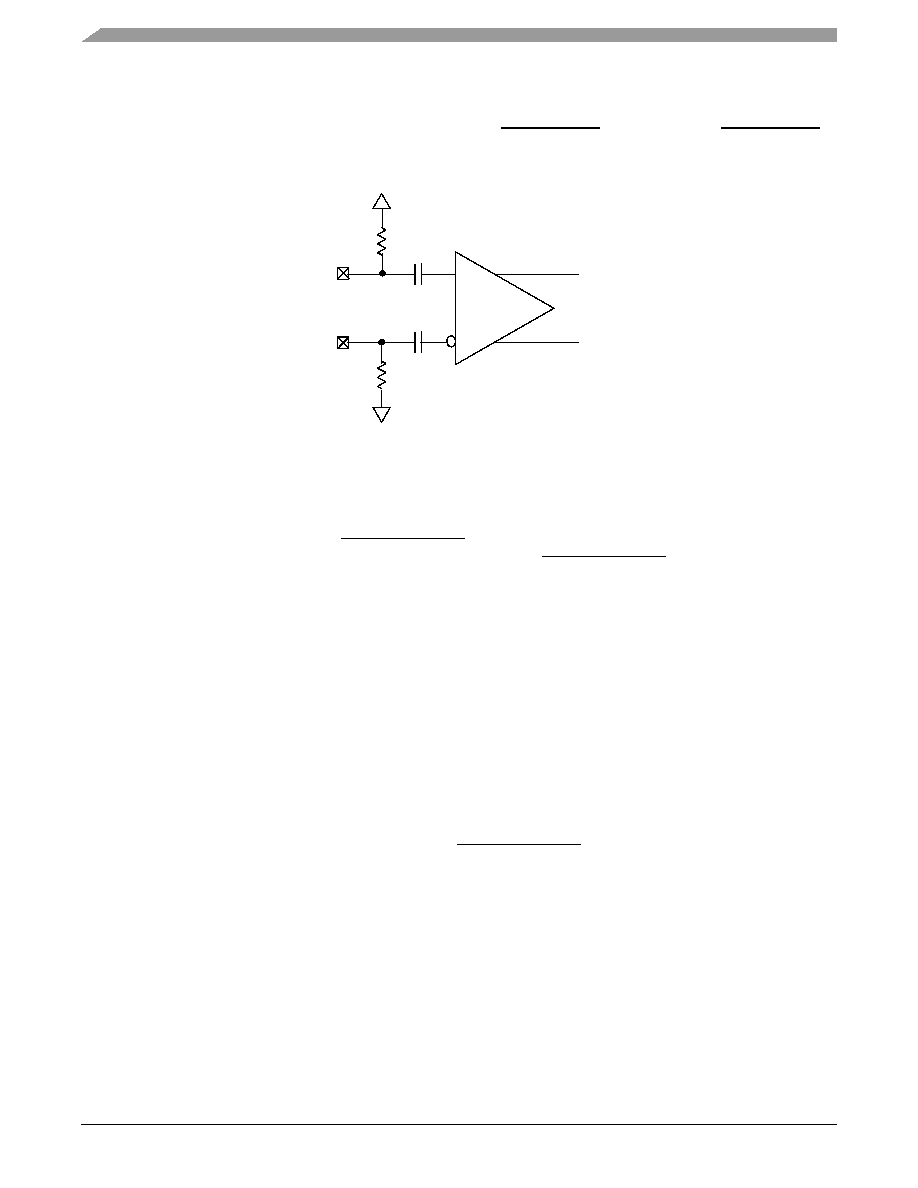
Figure 5 shows a receiver reference diagram of the SerDes reference clocks.
The characteristics of the clock signals are as follows:
The SerDes reference clock receiver reference circuit structure is as follows:
—The SR[1–2]_REF_CLK and SR[1–2]_REF_CLK are internally AC-coupled differential inputs as shown in
Figure 5. Each differential clock input (SR[1–2]_REF_CLK or SR[1–2]_REF_CLK) has on-chip 50-
Ω
termination to GNDSXC followed by on-chip AC-coupling.
— The external reference clock driver must be able to drive this termination.
— The SerDes reference clock input can be either differential or single-ended. Refer to the differential mode and
single-ended mode descriptions below for detailed requirements.
The maximum average current requirement also determines the common mode voltage range.
— When the SerDes reference clock differential inputs are DC coupled externally with the clock driver chip, the
maximum average current allowed for each input pin is 8 mA. In this case, the exact common mode input voltage
is not critical as long as it is within the range allowed by the maximum average current of 8 mA because the input
is AC-coupled on-chip.
— This current limitation sets the maximum common mode input voltage to be less than 0.4 V (0.4 V
/ 50 = 8 mA)
while the minimum common mode input level is 0.1 V above GNDSXC. For example, a clock with a 50/50 duty
cycle can be produced by a clock driver with output driven by its current source from 0 mA to 16 mA (0–0.8 V),
such that each phase of the differential input has a single-ended swing from 0 V to 800 mV with the common mode
voltage at 400 mV.
— If the device driving the SR[1–2]_REF_CLK and SR[1–2]_REF_CLK inputs cannot drive 50
Ω to GND
SXC DC or
the drive strength of the clock driver chip exceeds the maximum input current limitations, it must be AC-coupled
externally.
The input amplitude requirement is described in detail in the following sections.
Figure 5. Receiver of SerDes Reference Clocks
Input
Amp
50
Ω
50
Ω
SR[1–2]_REF_CLK
相關(guān)PDF資料 |
PDF描述 |
|---|---|
| MSC8154ETVT1000B | 0-BIT, OTHER DSP, PBGA783 |
| MSC8252TVT1000B | 0-BIT, OTHER DSP, PBGA783 |
| MSC8252SVT1000B | 0-BIT, OTHER DSP, PBGA783 |
| MSD1010LT3 | 100 mA, 15 V, PNP, Si, SMALL SIGNAL TRANSISTOR |
| MSD1010LT1 | 100 mA, 15 V, PNP, Si, SMALL SIGNAL TRANSISTOR |
相關(guān)代理商/技術(shù)參數(shù) |
參數(shù)描述 |
|---|---|
| MSC8154 | 制造商:FREESCALE 制造商全稱:Freescale Semiconductor, Inc 功能描述:Quad-Core Digital Signal Processor |
| MSC8154_11 | 制造商:FREESCALE 制造商全稱:Freescale Semiconductor, Inc 功能描述:Quad-Core Digital Signal processor |
| MSC8154E | 制造商:FREESCALE 制造商全稱:Freescale Semiconductor, Inc 功能描述:Quad-Core Digital Signal Processor with Security |
| MSC8154E_11 | 制造商:FREESCALE 制造商全稱:Freescale Semiconductor, Inc 功能描述:Quad-Core Digital Signal Processor with Security |
| MSC8154ESVT1000B | 功能描述:數(shù)字信號處理器和控制器 - DSP, DSC DSP StarCore 6-cores RoHS:否 制造商:Microchip Technology 核心:dsPIC 數(shù)據(jù)總線寬度:16 bit 程序存儲器大小:16 KB 數(shù)據(jù) RAM 大小:2 KB 最大時(shí)鐘頻率:40 MHz 可編程輸入/輸出端數(shù)量:35 定時(shí)器數(shù)量:3 設(shè)備每秒兆指令數(shù):50 MIPs 工作電源電壓:3.3 V 最大工作溫度:+ 85 C 封裝 / 箱體:TQFP-44 安裝風(fēng)格:SMD/SMT |
發(fā)布緊急采購,3分鐘左右您將得到回復(fù)。