- 您現(xiàn)在的位置:買賣IC網(wǎng) > PDF目錄359219 > MRF6V2150NBR1 (飛思卡爾半導(dǎo)體(中國)有限公司) RF Power Field-Effect Transistors N-Channel Enhancement-Mode Lateral MOSFETs PDF資料下載
參數(shù)資料
| 型號: | MRF6V2150NBR1 |
| 廠商: | 飛思卡爾半導(dǎo)體(中國)有限公司 |
| 英文描述: | RF Power Field-Effect Transistors N-Channel Enhancement-Mode Lateral MOSFETs |
| 中文描述: | 射頻功率場效應(yīng)晶體管N溝道增強型MOSFET的外側(cè) |
| 文件頁數(shù): | 2/13頁 |
| 文件大?。?/td> | 521K |
| 代理商: | MRF6V2150NBR1 |
2
RF Device Data
Freescale Semiconductor
MRF6V2150NR1 MRF6V2150NBR1
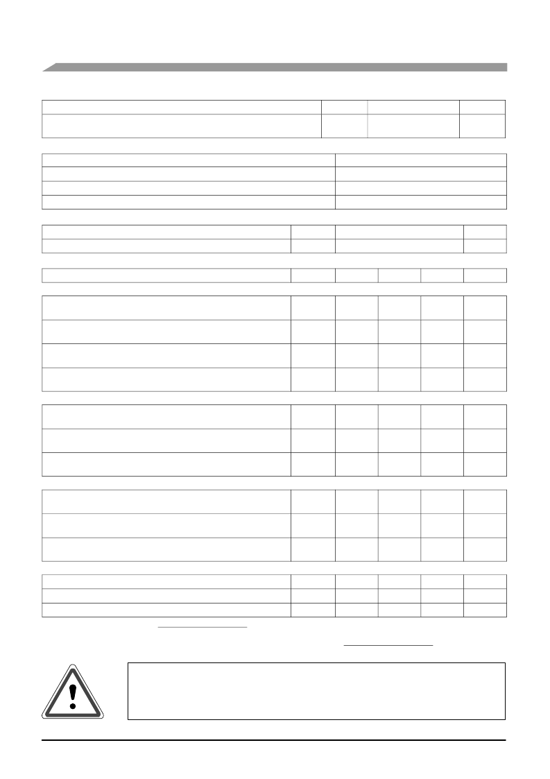
Table 2. Thermal Characteristics
Characteristic
Symbol
Value
(1,2)
Unit
Thermal Resistance, Junction to Case
Case Temperature 80
°
C, 150
W CW
R
θ
JC
0.24
°
C/W
Table 3. ESD Protection Characteristics
Test Methodology
Class
Human Body Model (per JESD22-A114)
2 (Minimum)
Machine Model (per EIA/JESD22-A115)
A (Minimum)
Charge Device Model (per JESD22-C101)
IV (Minimum)
Table 4. Moisture Sensitivity Level
Test Methodology
Rating
Package Peak Temperature
Unit
Per JESD 22-A113, IPC/JEDEC J-STD-020
3
260
°
C
Table 5. Electrical Characteristics
(T
C
= 25
°
C unless otherwise noted)
Characteristic
Symbol
Min
Typ
Max
Unit
Off Characteristics
Zero Gate Voltage Drain Leakage Current
(V
DS
= 100
Vdc, V
GS
= 0 Vdc)
I
DSS
—
—
2.5
mA
Zero Gate Voltage Drain Leakage Current
(V
DS
= 50 Vdc, V
GS
= 0 Vdc)
I
DSS
—
—
50
μ
Adc
Drain-Source Breakdown Voltage
(I
D
= 75 mA, V
GS
= 0 Vdc)
V
(BR)DSS
110
—
—
Vdc
Gate-Source Leakage Current
(V
GS
= 5 Vdc, V
DS
= 0 Vdc)
I
GSS
—
—
10
μ
Adc
On Characteristics
Gate Threshold Voltage
(V
DS
= 10 Vdc, I
D
= 400
μ
Adc)
V
GS(th)
1
1.62
3
Vdc
Gate Quiescent Voltage
(V
DD
= 50 Vdc, I
D
= 450 mAdc, Measured in Functional Test)
V
GS(Q)
1.5
2.6
3.5
Vdc
Drain-Source On-Voltage
(V
GS
= 10 Vdc, I
D
= 1
Adc)
V
DS(on)
—
0.26
—
Vdc
Dynamic Characteristics
Reverse Transfer Capacitance
(V
DS
= 50
Vdc
±
30 mV(rms)ac @ 1 MHz, V
GS
= 0 Vdc)
C
rss
—
1.6
—
pF
Output Capacitance
(V
DS
= 50
Vdc
±
30 mV(rms)ac @ 1 MHz, V
GS
= 0 Vdc)
C
oss
—
93
—
pF
Input Capacitance
(V
DS
= 50
Vdc
±
30 mV(rms)ac @ 1 MHz, V
GS
= 0 Vdc)
C
iss
—
163
—
pF
Functional Tests
(In Freescale Test Fixture, 50 ohm system) V
DD
= 50 Vdc, I
DQ
= 450 mA, P
out
= 150 W, f = 220 MHz, CW
Power Gain
G
ps
23.5
25
26.5
dB
Drain Efficiency
η
D
66
68.3
—
%
Input Return Loss
IRL
—
-17
-9
dB
1. MTTF calculator available at http://www.freescale.com/rf. Select Tools/Software/Application Software/Calculators to access the MTTF
calculators by product.
2. Refer to AN1955,
Thermal Measurement Methodology of RF Power Amplifiers.
Go to http://www.freescale.com/rf.
Select Documentation/Application Notes - AN1955.
ATTENTION: The MRF6V2150N and MRF6V2150NB are high power devices and special considerations
must be followed in board design and mounting. Incorrect mounting can lead to internal temperatures which
exceed the maximum allowable operating junction temperature. Refer to Freescale Application Note AN3263
(for bolt down mounting) or AN1907 (for solder reflow mounting)
PRIOR TO STARTING SYSTEM DESIGN
to
ensure proper mounting of these devices.
相關(guān)PDF資料 |
PDF描述 |
|---|---|
| MRF6V2150N | N-Channel Enhancement-Mode Lateral MOSFETs |
| MRF6V2300NBR1 | RF Power Field Effect Transistors N-Channel Enhancement-Mode Lateral MOSFETs |
| MRF6V2300N | N-Channel Enhancement-Mode Lateral MOSFETs |
| MRF6VP11KHR6 | RF Power Field Effect Transistor N-Channel Enhancement-Mode Lateral MOSFET |
| MRF7S18170H | RF Power Field Effect Transistors (N-Channel Enhancement-Mode Lateral MOSFETs) |
相關(guān)代理商/技術(shù)參數(shù) |
參數(shù)描述 |
|---|---|
| MRF6V2150NBR5 | 功能描述:射頻MOSFET電源晶體管 VHV6 150W Latrl N-Ch SE Broadband MOSFET RoHS:否 制造商:Freescale Semiconductor 配置:Single 晶體管極性: 頻率:1800 MHz to 2000 MHz 增益:27 dB 輸出功率:100 W 汲極/源極擊穿電壓: 漏極連續(xù)電流: 閘/源擊穿電壓: 最大工作溫度: 封裝 / 箱體:NI-780-4 封裝:Tray |
| MRF6V2150NBR5-CUT TAPE | 制造商:Freescale 功能描述:MRF6V2150 Series 10 - 450 MHz 150 W 50 V N-Channel RF Power MOSFET - TO-272 |
| MRF6V2150NR1 | 功能描述:射頻MOSFET電源晶體管 VHV6 150W RoHS:否 制造商:Freescale Semiconductor 配置:Single 晶體管極性: 頻率:1800 MHz to 2000 MHz 增益:27 dB 輸出功率:100 W 汲極/源極擊穿電壓: 漏極連續(xù)電流: 閘/源擊穿電壓: 最大工作溫度: 封裝 / 箱體:NI-780-4 封裝:Tray |
| MRF6V2150NR1_08 | 制造商:FREESCALE 制造商全稱:Freescale Semiconductor, Inc 功能描述:RF Power Field-Effect Transistors N-Channel Enhancement-Mode Lateral MOSFETs |
| MRF6V2150NR1-CUT TAPE | 制造商:Freescale 功能描述:RF POWER MOSFET 10-450 MHz, 150 W, 50 V |
發(fā)布緊急采購,3分鐘左右您將得到回復(fù)。