- 您現(xiàn)在的位置:買賣IC網(wǎng) > PDF目錄45379 > MQ80C32-12P883D (TEMIC SEMICONDUCTORS) 8-BIT, 12 MHz, MICROCONTROLLER, CQFP44 PDF資料下載
參數(shù)資料
| 型號: | MQ80C32-12P883D |
| 廠商: | TEMIC SEMICONDUCTORS |
| 元件分類: | 微控制器/微處理器 |
| 英文描述: | 8-BIT, 12 MHz, MICROCONTROLLER, CQFP44 |
| 文件頁數(shù): | 47/286頁 |
| 文件大小: | 9413K |
| 代理商: | MQ80C32-12P883D |
第1頁第2頁第3頁第4頁第5頁第6頁第7頁第8頁第9頁第10頁第11頁第12頁第13頁第14頁第15頁第16頁第17頁第18頁第19頁第20頁第21頁第22頁第23頁第24頁第25頁第26頁第27頁第28頁第29頁第30頁第31頁第32頁第33頁第34頁第35頁第36頁第37頁第38頁第39頁第40頁第41頁第42頁第43頁第44頁第45頁第46頁當(dāng)前第47頁第48頁第49頁第50頁第51頁第52頁第53頁第54頁第55頁第56頁第57頁第58頁第59頁第60頁第61頁第62頁第63頁第64頁第65頁第66頁第67頁第68頁第69頁第70頁第71頁第72頁第73頁第74頁第75頁第76頁第77頁第78頁第79頁第80頁第81頁第82頁第83頁第84頁第85頁第86頁第87頁第88頁第89頁第90頁第91頁第92頁第93頁第94頁第95頁第96頁第97頁第98頁第99頁第100頁第101頁第102頁第103頁第104頁第105頁第106頁第107頁第108頁第109頁第110頁第111頁第112頁第113頁第114頁第115頁第116頁第117頁第118頁第119頁第120頁第121頁第122頁第123頁第124頁第125頁第126頁第127頁第128頁第129頁第130頁第131頁第132頁第133頁第134頁第135頁第136頁第137頁第138頁第139頁第140頁第141頁第142頁第143頁第144頁第145頁第146頁第147頁第148頁第149頁第150頁第151頁第152頁第153頁第154頁第155頁第156頁第157頁第158頁第159頁第160頁第161頁第162頁第163頁第164頁第165頁第166頁第167頁第168頁第169頁第170頁第171頁第172頁第173頁第174頁第175頁第176頁第177頁第178頁第179頁第180頁第181頁第182頁第183頁第184頁第185頁第186頁第187頁第188頁第189頁第190頁第191頁第192頁第193頁第194頁第195頁第196頁第197頁第198頁第199頁第200頁第201頁第202頁第203頁第204頁第205頁第206頁第207頁第208頁第209頁第210頁第211頁第212頁第213頁第214頁第215頁第216頁第217頁第218頁第219頁第220頁第221頁第222頁第223頁第224頁第225頁第226頁第227頁第228頁第229頁第230頁第231頁第232頁第233頁第234頁第235頁第236頁第237頁第238頁第239頁第240頁第241頁第242頁第243頁第244頁第245頁第246頁第247頁第248頁第249頁第250頁第251頁第252頁第253頁第254頁第255頁第256頁第257頁第258頁第259頁第260頁第261頁第262頁第263頁第264頁第265頁第266頁第267頁第268頁第269頁第270頁第271頁第272頁第273頁第274頁第275頁第276頁第277頁第278頁第279頁第280頁第281頁第282頁第283頁第284頁第285頁第286頁
140
8183F–AVR–06/12
ATtiny24A/44A/84A
In order to avoid distortion from unpredictable signal convolution, signal components higher than
the Nyquist frequency (f
ADC/2) should not be present. The user is advised to remove high fre-
quency components with a low-pass filter before applying the signals as inputs to the ADC.
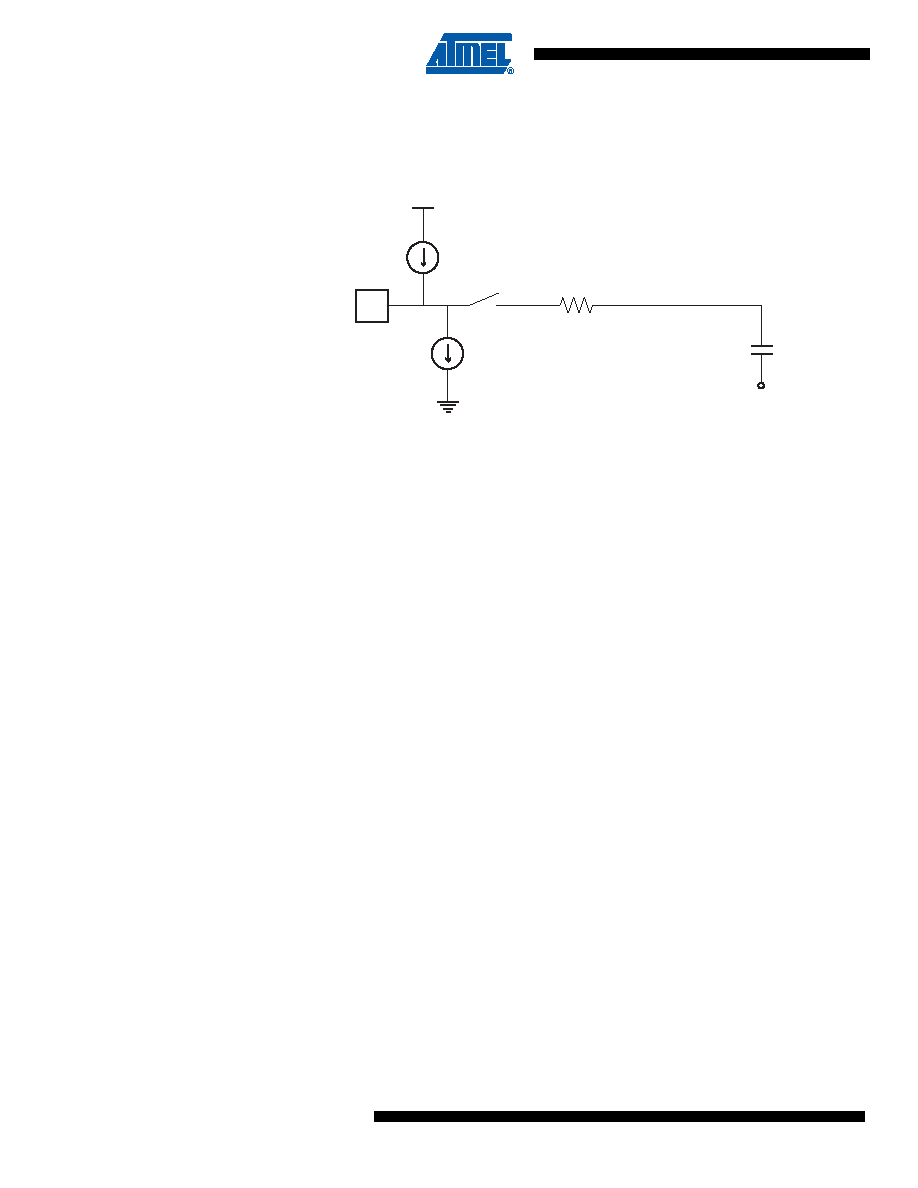
Figure 16-8.
Analog Input Circuitry
Note:
The capacitor in the figure depicts the total capacitance, including the sample/hold capacitor and
any stray or parasitic capacitance inside the device. The value given is worst case.
16.9
Noise Canceling Techniques
Digital circuitry inside and outside the device generates EMI which might affect the accuracy of
analog measurements. When conversion accuracy is critical, the noise level can be reduced by
applying the following techniques:
Keep analog signal paths as short as possible.
Make sure analog tracks run over the analog ground plane.
Keep analog tracks well away from high-speed switching digital tracks.
If any port pin is used as a digital output, it mustn’t switch while a conversion is in progress.
Place bypass capacitors as close to V
CC and GND pins as possible.
Where high ADC accuracy is required it is recommended to use ADC Noise Reduction Mode, as
described in Section 16.7 on page 139. This is especially the case when system clock frequency
is above 1 MHz, or when the ADC is used for reading the internal temperature sensor, as
described in Section 16.12 on page 143. A good system design with properly placed, external
bypass capacitors does reduce the need for using ADC Noise Reduction Mode
16.10 ADC Accuracy Definitions
An n-bit single-ended ADC converts a voltage linearly between GND and V
REF in 2
n steps
(LSBs). The lowest code is read as 0, and the highest code is read as 2
n-1.
Several parameters describe the deviation from the ideal behavior, as follows:
ADCn
IIH
1..100 k
ohm
CS/H = 14 pF
VCC/2
IIL
相關(guān)PDF資料 |
PDF描述 |
|---|---|
| MD80C52CXXX-25SB | 8-BIT, MROM, 25 MHz, MICROCONTROLLER, CDIP40 |
| MR80C52XXX-36SBR | 8-BIT, MROM, 36 MHz, MICROCONTROLLER, CQCC44 |
| MR83C154CXXX-16/883 | 8-BIT, MROM, 16 MHz, MICROCONTROLLER, CQCC44 |
| MQ83C154DTXXX-16/883R | 8-BIT, MROM, 16 MHz, MICROCONTROLLER, CQFP44 |
| MQ83C154DTXXX-25P883 | 8-BIT, MROM, 25 MHz, MICROCONTROLLER, CQFP44 |
相關(guān)代理商/技術(shù)參數(shù) |
參數(shù)描述 |
|---|---|
| MQ82370-20 | 制造商:Rochester Electronics LLC 功能描述:- Bulk |
| MQ8238020 | 制造商:Intel 功能描述:CONTROLLER: OTHER |
| MQ82380-20 | 制造商:Rochester Electronics LLC 功能描述:- Bulk |
| MQ82380-20/R | 制造商:Rochester Electronics LLC 功能描述: |
| MQ82592 | 制造商:Rochester Electronics LLC 功能描述:- Bulk |
發(fā)布緊急采購,3分鐘左右您將得到回復(fù)。