- 您現(xiàn)在的位置:買賣IC網 > PDF目錄98029 > MPS650RL1 (ON SEMICONDUCTOR) 2000 mA, 40 V, NPN, Si, SMALL SIGNAL TRANSISTOR, TO-92 PDF資料下載
參數(shù)資料
| 型號: | MPS650RL1 |
| 廠商: | ON SEMICONDUCTOR |
| 元件分類: | 小信號晶體管 |
| 英文描述: | 2000 mA, 40 V, NPN, Si, SMALL SIGNAL TRANSISTOR, TO-92 |
| 封裝: | PLASTIC, TO-226AA, 3 PIN |
| 文件頁數(shù): | 5/34頁 |
| 文件大?。?/td> | 342K |
| 代理商: | MPS650RL1 |
第1頁第2頁第3頁第4頁當前第5頁第6頁第7頁第8頁第9頁第10頁第11頁第12頁第13頁第14頁第15頁第16頁第17頁第18頁第19頁第20頁第21頁第22頁第23頁第24頁第25頁第26頁第27頁第28頁第29頁第30頁第31頁第32頁第33頁第34頁
7–11
Surface Mount Information
Motorola Small–Signal Transistors, FETs and Diodes Device Data
SOLDERING PRECAUTIONS
The melting temperature of solder is higher than the rated
temperature of the device. When the entire device is heated
to a high temperature, failure to complete soldering within a
short time could result in device failure. Therefore, the
following items should always be observed in order to mini-
mize the thermal stress to which the devices are subjected.
Always preheat the device.
The delta temperature between the preheat and soldering
should be 100
°C or less.*
When preheating and soldering, the temperature of the
leads and the case must not exceed the maximum
temperature ratings as shown on the data sheet. When
using infrared heating with the reflow soldering method,
the difference should be a maximum of 10
°C.
The soldering temperature and time should not exceed
260
°C for more than 10 seconds.
When shifting from preheating to soldering, the maximum
temperature gradient shall be 5
°C or less.
After soldering has been completed, the device should be
allowed to cool naturally for at least three minutes.
Gradual cooling should be used since the use of forced
cooling will increase the temperature gradient and will
result in latent failure due to mechanical stress.
Mechanical stress or shock should not be applied during
cooling.
* Soldering a device without preheating can cause excessive
thermal shock and stress which can result in damage to the
device.
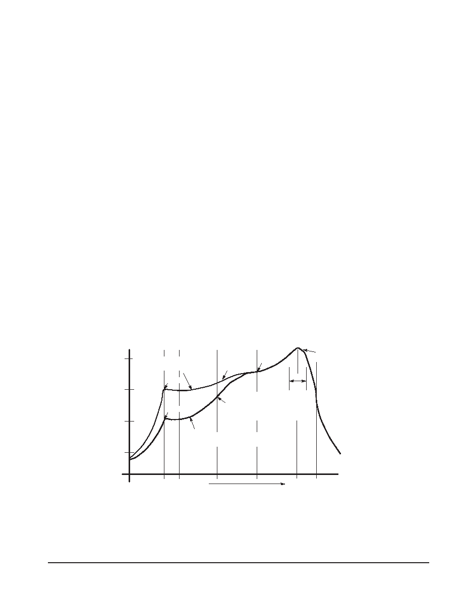
TYPICAL SOLDER HEATING PROFILE
For any given circuit board, there will be a group of control
settings that will give the desired heat pattern. The operator
must set temperatures for several heating zones and a figure
for belt speed. Taken together, these control settings make
up a heating “profile” for that particular circuit board. On
machines controlled by a computer, the computer remem-
bers these profiles from one operating session to the next.
Figure 2 shows a typical heating profile for use when
soldering a surface mount device to a printed circuit board.
This profile will vary among soldering systems, but it is a
good starting point. Factors that can affect the profile include
the type of soldering system in use, density and types of
components on the board, type of solder used, and the type
of board or substrate material being used. This profile shows
temperature versus time. The line on the graph shows the
actual temperature that might be experienced on the surface
of a test board at or near a central solder joint. The two
profiles are based on a high density and a low density board.
The Vitronics SMD310 convection/infrared reflow soldering
system was used to generate this profile. The type of solder
used was 62/36/2 Tin Lead Silver with a melting point
between 177 –189
°C. When this type of furnace is used for
solder reflow work, the circuit boards and solder joints tend to
heat first. The components on the board are then heated by
conduction. The circuit board, because it has a large surface
area, absorbs the thermal energy more efficiently, then
distributes this energy to the components. Because of this
effect, the main body of a component may be up to 30
degrees cooler than the adjacent solder joints.
STEP 1
PREHEAT
ZONE 1
“RAMP”
STEP 2
VENT
“SOAK”
STEP 3
HEATING
ZONES 2 & 5
“RAMP”
STEP 4
HEATING
ZONES 3 & 6
“SOAK”
STEP 5
HEATING
ZONES 4 & 7
“SPIKE”
STEP 6
VENT
STEP 7
COOLING
200
°C
150
°C
100
°C
50
°C
TIME (3 TO 7 MINUTES TOTAL)
TMAX
SOLDER IS LIQUID FOR
40 TO 80 SECONDS
(DEPENDING ON
MASS OF ASSEMBLY)
205
° TO 219°C
PEAK AT
SOLDER JOINT
DESIRED CURVE FOR LOW
MASS ASSEMBLIES
100
°C
150
°C
160
°C
170
°C
140
°C
Figure 2. Typical Solder Heating Profile
DESIRED CURVE FOR HIGH
MASS ASSEMBLIES
相關PDF資料 |
PDF描述 |
|---|---|
| MPS651RLRE | 2000 mA, 60 V, NPN, Si, SMALL SIGNAL TRANSISTOR, TO-92 |
| MPS651RL1 | 2000 mA, 60 V, NPN, Si, SMALL SIGNAL TRANSISTOR, TO-92 |
| MPS750RL1 | 2000 mA, 40 V, PNP, Si, SMALL SIGNAL TRANSISTOR, TO-92 |
| MPS751RLRE | 2000 mA, 60 V, PNP, Si, SMALL SIGNAL TRANSISTOR, TO-92 |
| MPS650RLRM | 2000 mA, 40 V, NPN, Si, SMALL SIGNAL TRANSISTOR, TO-92 |
相關代理商/技術參數(shù) |
參數(shù)描述 |
|---|---|
| MPS650RLRA | 功能描述:兩極晶體管 - BJT 2A 60V NPN RoHS:否 制造商:STMicroelectronics 配置: 晶體管極性:PNP 集電極—基極電壓 VCBO: 集電極—發(fā)射極最大電壓 VCEO:- 40 V 發(fā)射極 - 基極電壓 VEBO:- 6 V 集電極—射極飽和電壓: 最大直流電集電極電流: 增益帶寬產品fT: 直流集電極/Base Gain hfe Min:100 A 最大工作溫度: 安裝風格:SMD/SMT 封裝 / 箱體:PowerFLAT 2 x 2 |
| MPS650RLRAG | 功能描述:兩極晶體管 - BJT 2A 60V NPN RoHS:否 制造商:STMicroelectronics 配置: 晶體管極性:PNP 集電極—基極電壓 VCBO: 集電極—發(fā)射極最大電壓 VCEO:- 40 V 發(fā)射極 - 基極電壓 VEBO:- 6 V 集電極—射極飽和電壓: 最大直流電集電極電流: 增益帶寬產品fT: 直流集電極/Base Gain hfe Min:100 A 最大工作溫度: 安裝風格:SMD/SMT 封裝 / 箱體:PowerFLAT 2 x 2 |
| MPS650ZL1 | 功能描述:兩極晶體管 - BJT 2A 60V NPN RoHS:否 制造商:STMicroelectronics 配置: 晶體管極性:PNP 集電極—基極電壓 VCBO: 集電極—發(fā)射極最大電壓 VCEO:- 40 V 發(fā)射極 - 基極電壓 VEBO:- 6 V 集電極—射極飽和電壓: 最大直流電集電極電流: 增益帶寬產品fT: 直流集電極/Base Gain hfe Min:100 A 最大工作溫度: 安裝風格:SMD/SMT 封裝 / 箱體:PowerFLAT 2 x 2 |
| MPS650ZL1G | 功能描述:兩極晶體管 - BJT 2A 60V NPN RoHS:否 制造商:STMicroelectronics 配置: 晶體管極性:PNP 集電極—基極電壓 VCBO: 集電極—發(fā)射極最大電壓 VCEO:- 40 V 發(fā)射極 - 基極電壓 VEBO:- 6 V 集電極—射極飽和電壓: 最大直流電集電極電流: 增益帶寬產品fT: 直流集電極/Base Gain hfe Min:100 A 最大工作溫度: 安裝風格:SMD/SMT 封裝 / 箱體:PowerFLAT 2 x 2 |
| MPS651 | 功能描述:兩極晶體管 - BJT NPN Transistor Medium Power RoHS:否 制造商:STMicroelectronics 配置: 晶體管極性:PNP 集電極—基極電壓 VCBO: 集電極—發(fā)射極最大電壓 VCEO:- 40 V 發(fā)射極 - 基極電壓 VEBO:- 6 V 集電極—射極飽和電壓: 最大直流電集電極電流: 增益帶寬產品fT: 直流集電極/Base Gain hfe Min:100 A 最大工作溫度: 安裝風格:SMD/SMT 封裝 / 箱體:PowerFLAT 2 x 2 |
發(fā)布緊急采購,3分鐘左右您將得到回復。