- 您現(xiàn)在的位置:買賣IC網(wǎng) > PDF目錄9017 > MPC9772FAR2 (IDT, Integrated Device Technology Inc)IC PLL CLK GEN 1:12 3.3V 52-LQFP PDF資料下載
參數(shù)資料
| 型號: | MPC9772FAR2 |
| 廠商: | IDT, Integrated Device Technology Inc |
| 文件頁數(shù): | 16/17頁 |
| 文件大?。?/td> | 0K |
| 描述: | IC PLL CLK GEN 1:12 3.3V 52-LQFP |
| 標(biāo)準(zhǔn)包裝: | 1,500 |
| 類型: | PLL 時(shí)鐘發(fā)生器 |
| PLL: | 帶旁路 |
| 輸入: | LVCMOS,晶體 |
| 輸出: | LVCMOS |
| 電路數(shù): | 1 |
| 比率 - 輸入:輸出: | 3:12 |
| 差分 - 輸入:輸出: | 無/無 |
| 頻率 - 最大: | 240MHz |
| 除法器/乘法器: | 是/無 |
| 電源電壓: | 3.135 V ~ 3.465 V |
| 工作溫度: | 0°C ~ 70°C |
| 安裝類型: | 表面貼裝 |
| 封裝/外殼: | 52-LQFP |
| 供應(yīng)商設(shè)備封裝: | 52-TQFP(10x10) |
| 包裝: | 帶卷 (TR) |
MPC9772 REVISION 7 JANUARY 8, 2013
8
2013 Integrated Device Technology, Inc.
MPC9772 Data Sheet
3.3V 1:12 LVCMOS PLL CLOCK GENERATOR
APPLICATIONS INFORMATION
MPC9772 Configurations
Configuring the MPC9772 amounts to properly configuring
the internal dividers to produce the desired output
frequencies. The output frequency can be represented by
this formula:
where fREF is the reference frequency of the selected input
clock source (CCLKO, CCLK1 or XTAL interface), M is the
PLL feedback divider and N is a output divider. The PLL
feedback divider is configured by the FSEL_FB[2:0] and the
output dividers are individually configured for each output
bank by the FSEL_A[1:0], FSEL_B[1:0] and FSEL_C[1:0]
inputs.
The reference frequency fREF and the selection of the
feedback-divider M is limited by the specified VCO frequency
range. fREF and M must be configured to match the VCO
frequency range of 200 to 480 MHz in order to achieve stable
PLL operation:
fVCO,MIN (fREF VCO_SEL M) fVCO,MAX
The PLL post-divider VCO_SEL is either a divide-by-one
or a divide-by-two and can be used to situate the VCO into
the specified frequency range. This divider is controlled by
the VCO_SEL pin. VCO_SEL effectively extends the usable
input frequency range while it has no effect on the output to
reference frequency ratio.
The output frequency for each bank can be derived from
the VCO frequency and output divider:
fQA[0:3] = fVCO (VCO_SEL NA)
fQB[0:3] = fVCO (VCO_SEL NB)
fQC[0:3] = fVCO (VCO_SEL NC)
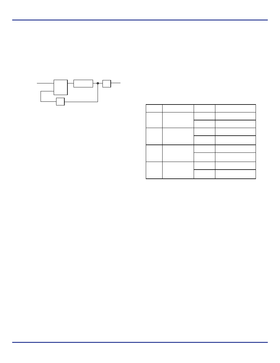
Table 11 shows the various PLL feedback and output
configurations for the MPC9772:
VCO_SEL
M
N
fREF
fOUT
fOUT = fREF M N
PLL
Table 11. MPC9772 Divider
Divider
Function
VCO_SEL
Values
M
PLL feedback
FSEL_FB[0:3]
1
4, 6, 8, 10, 12, 16
2
8, 12, 16, 20, 24, 32, 40
NA
Bank A Output
Divider
FSEL_A[0:1]
1
4, 6, 8, 12
2
8, 12, 16, 24
NB
Bank B Output
Divider
FSEL_B[0:1]
1
4, 6, 8, 10
2
8, 12, 16, 20
NC
Bank C Output
Divider
FSEL_C[0:1]
1
2, 4, 6, 8
2
4, 8, 12, 16
相關(guān)PDF資料 |
PDF描述 |
|---|---|
| VE-201-MY-F4 | CONVERTER MOD DC/DC 12V 50W |
| MPC9772AER2 | IC PLL CLK GEN 1:12 3.3V 52-LQFP |
| VI-J7J-MZ-F2 | CONVERTER MOD DC/DC 36V 25W |
| VE-201-MY-F2 | CONVERTER MOD DC/DC 12V 50W |
| IDT23S08E-5HDCI8 | IC CLK MULT PLL HI DRV 16-SOIC |
相關(guān)代理商/技術(shù)參數(shù) |
參數(shù)描述 |
|---|---|
| MPC9773 | 制造商:FREESCALE 制造商全稱:Freescale Semiconductor, Inc 功能描述:3.3 V 1:12 LVCMOS PLL Clock Generator |
| MPC9773AE | 功能描述:時(shí)鐘發(fā)生器及支持產(chǎn)品 FSL 1-12 LVCMOS/LVPE CL to LVCMOS PLL Clo RoHS:否 制造商:Silicon Labs 類型:Clock Generators 最大輸入頻率:14.318 MHz 最大輸出頻率:166 MHz 輸出端數(shù)量:16 占空比 - 最大:55 % 工作電源電壓:3.3 V 工作電源電流:1 mA 最大工作溫度:+ 85 C 安裝風(fēng)格:SMD/SMT 封裝 / 箱體:QFN-56 |
| MPC9773AER2 | 功能描述:時(shí)鐘發(fā)生器及支持產(chǎn)品 FSL 1-12 LVCMOS/LVPE CL to LVCMOS PLL Clo RoHS:否 制造商:Silicon Labs 類型:Clock Generators 最大輸入頻率:14.318 MHz 最大輸出頻率:166 MHz 輸出端數(shù)量:16 占空比 - 最大:55 % 工作電源電壓:3.3 V 工作電源電流:1 mA 最大工作溫度:+ 85 C 安裝風(fēng)格:SMD/SMT 封裝 / 箱體:QFN-56 |
| MPC9773FA | 功能描述:鎖相環(huán) - PLL 3.3V 240MHz Clock Generator RoHS:否 制造商:Silicon Labs 類型:PLL Clock Multiplier 電路數(shù)量:1 最大輸入頻率:710 MHz 最小輸入頻率:0.002 MHz 輸出頻率范圍:0.002 MHz to 808 MHz 電源電壓-最大:3.63 V 電源電壓-最小:1.71 V 最大工作溫度:+ 85 C 最小工作溫度:- 40 C 封裝 / 箱體:QFN-36 封裝:Tray |
| MPC9773FAR2 | 制造商:Integrated Device Technology Inc 功能描述:PLL Clock Driver Single 52-Pin LQFP T/R 制造商:Integrated Device Technology Inc 功能描述:MPC9773FAR2 - Tape and Reel |
發(fā)布緊急采購,3分鐘左右您將得到回復(fù)。