- 您現(xiàn)在的位置:買賣IC網(wǎng) > PDF目錄1955 > MPC8377CVRANGA (Freescale Semiconductor)MPU POWERQUICC II 800MHZ 689PBGA PDF資料下載
參數(shù)資料
| 型號(hào): | MPC8377CVRANGA |
| 廠商: | Freescale Semiconductor |
| 文件頁(yè)數(shù): | 37/127頁(yè) |
| 文件大?。?/td> | 0K |
| 描述: | MPU POWERQUICC II 800MHZ 689PBGA |
| 標(biāo)準(zhǔn)包裝: | 27 |
| 系列: | MPC83xx |
| 處理器類型: | 32-位 MPC83xx PowerQUICC II Pro |
| 速度: | 800MHz |
| 電壓: | 1.05V |
| 安裝類型: | 表面貼裝 |
| 封裝/外殼: | 689-BBGA 裸露焊盤 |
| 供應(yīng)商設(shè)備封裝: | 689-TEPBGA II(31x31) |
| 包裝: | 托盤 |
第1頁(yè)第2頁(yè)第3頁(yè)第4頁(yè)第5頁(yè)第6頁(yè)第7頁(yè)第8頁(yè)第9頁(yè)第10頁(yè)第11頁(yè)第12頁(yè)第13頁(yè)第14頁(yè)第15頁(yè)第16頁(yè)第17頁(yè)第18頁(yè)第19頁(yè)第20頁(yè)第21頁(yè)第22頁(yè)第23頁(yè)第24頁(yè)第25頁(yè)第26頁(yè)第27頁(yè)第28頁(yè)第29頁(yè)第30頁(yè)第31頁(yè)第32頁(yè)第33頁(yè)第34頁(yè)第35頁(yè)第36頁(yè)當(dāng)前第37頁(yè)第38頁(yè)第39頁(yè)第40頁(yè)第41頁(yè)第42頁(yè)第43頁(yè)第44頁(yè)第45頁(yè)第46頁(yè)第47頁(yè)第48頁(yè)第49頁(yè)第50頁(yè)第51頁(yè)第52頁(yè)第53頁(yè)第54頁(yè)第55頁(yè)第56頁(yè)第57頁(yè)第58頁(yè)第59頁(yè)第60頁(yè)第61頁(yè)第62頁(yè)第63頁(yè)第64頁(yè)第65頁(yè)第66頁(yè)第67頁(yè)第68頁(yè)第69頁(yè)第70頁(yè)第71頁(yè)第72頁(yè)第73頁(yè)第74頁(yè)第75頁(yè)第76頁(yè)第77頁(yè)第78頁(yè)第79頁(yè)第80頁(yè)第81頁(yè)第82頁(yè)第83頁(yè)第84頁(yè)第85頁(yè)第86頁(yè)第87頁(yè)第88頁(yè)第89頁(yè)第90頁(yè)第91頁(yè)第92頁(yè)第93頁(yè)第94頁(yè)第95頁(yè)第96頁(yè)第97頁(yè)第98頁(yè)第99頁(yè)第100頁(yè)第101頁(yè)第102頁(yè)第103頁(yè)第104頁(yè)第105頁(yè)第106頁(yè)第107頁(yè)第108頁(yè)第109頁(yè)第110頁(yè)第111頁(yè)第112頁(yè)第113頁(yè)第114頁(yè)第115頁(yè)第116頁(yè)第117頁(yè)第118頁(yè)第119頁(yè)第120頁(yè)第121頁(yè)第122頁(yè)第123頁(yè)第124頁(yè)第125頁(yè)第126頁(yè)第127頁(yè)
MPC8377E PowerQUICC II Pro Processor Hardware Specifications, Rev. 8
Freescale Semiconductor
17
6.1
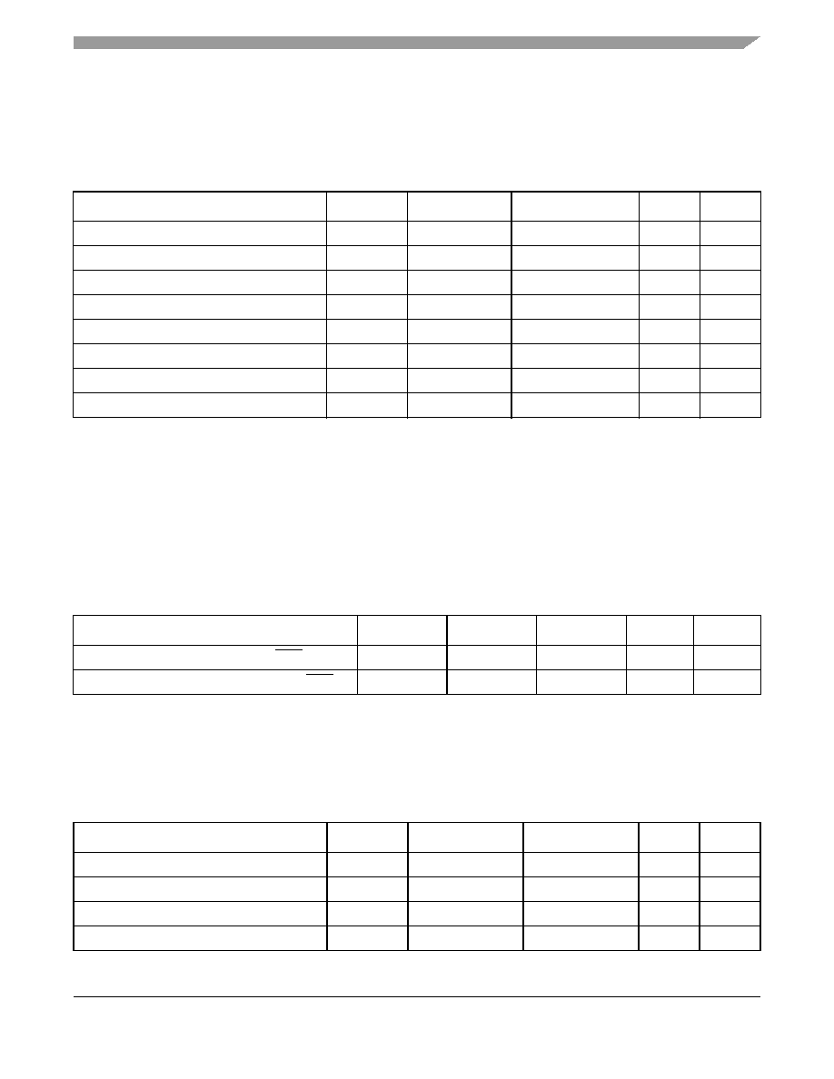
DDR1 and DDR2 SDRAM DC Electrical Characteristics
This table provides the recommended operating conditions for the DDR2 SDRAM component(s) of the
device when GVDD(typ) = 1.8 V.
This table provides the recommended operating conditions for the DDR SDRAM component(s) when
GVDD(typ) = 2.5 V.
Table 13. DDR2 SDRAM DC Electrical Characteristics for GVDD(typ) = 1.8 V
Parameter
Symbol
Min
Max
Unit
Note
I/O supply voltage
GVDD
1.71
1.89
V
I/O reference voltage
MVREF
0.49
× GVDD
0.51
× GVDD
I/O termination voltage
VTT
MVREF –0.04
MVREF +0.04
V
Input high voltage
VIH
MVREF + 0.140
GVDD +0.3
V
—
Input low voltage
VIL
–0.3
MVREF – 0.140
V
—
Output leakage current
IOZ
–50
50
μA4
Output high current (VOUT =1.40V)
IOH
–13.4
—
mA
—
Output low current (VOUT =0.3 V)
IOL
13.4
—
mA
—
Notes:
1. GVDD is expected to be within 50 mV of the DRAM GVDD at all times.
2. MVREF is expected to be equal to 0.5 × GVDD, and to track GVDD DC variations as measured at the receiver. Peak-to-peak
noise on MVREF may not exceed ±2% of the DC value.
3. VTT is not applied directly to the device. It is the supply to which far end signal termination is made and is expected to be
equal to MVREF. This rail should track variations in the DC level of MVREF.
4. Output leakage is measured with all outputs disabled, 0 V
≤ V
OUT ≤ GVDD.
5. See AN3665, “MPC837xE Design Checklist,” for proper DDR termination.
Table 14. DDR2 SDRAM Capacitance for GVDD(typ) = 1.8 V
Parameter
Symbol
Min
Max
Unit
Note
Input/output capacitance: DQ, DQS, DQS
CIO
68
pF
Delta input/output capacitance: DQ, DQS, DQS
CDIO
—0.5
pF
Note:
1. This parameter is sampled. GVDD = 1.8 V ± 0.090 V, f = 1 MHz, TA = 25°C, VOUT = GVDD/2, VOUT (peak-to-peak) = 0.2 V.
Table 15. DDR SDRAM DC Electrical Characteristics for GVDD (typ) = 2.5 V
Parameter
Symbol
Min
Max
Unit
Note
I/O supply voltage
GVDD
2.375
2.625
V
I/O reference voltage
MVREF
0.49
× GVDD
0.51
× GVDD
I/O termination voltage
VTT
MVREF – 0.04
MVREF + 0.04
V
Input high voltage
VIH
MVREF + 0.18
GVDD + 0.3
V
—
相關(guān)PDF資料 |
PDF描述 |
|---|---|
| MPC8377EVRANG | MPU POWERQUICC II PRO 689-PBGA |
| MPC8378CVRANGA | MPU POWERQUICC II 800MHZ 689PBGA |
| MPC8378VRAJF | MPU POWERQUICC II PRO 689-PBGA |
| MPC8379CVRANGA | MPU POWERQUICC II 800MHZ 689PBGA |
| MPC8379VRANG | MPU POWERQUICC II PRO 689-PBGA |
相關(guān)代理商/技術(shù)參數(shù) |
參數(shù)描述 |
|---|---|
| MPC8377CZQAFDA | 制造商:FREESCALE 制造商全稱:Freescale Semiconductor, Inc 功能描述:PowerQUICC? II Pro Processor Hardware Specifications |
| MPC8377CZQAFFA | 制造商:FREESCALE 制造商全稱:Freescale Semiconductor, Inc 功能描述:PowerQUICC? II Pro Processor Hardware Specifications |
| MPC8377CZQAFGA | 制造商:FREESCALE 制造商全稱:Freescale Semiconductor, Inc 功能描述:PowerQUICC? II Pro Processor Hardware Specifications |
| MPC8377CZQAGDA | 制造商:FREESCALE 制造商全稱:Freescale Semiconductor, Inc 功能描述:PowerQUICC? II Pro Processor Hardware Specifications |
| MPC8377CZQAGFA | 制造商:FREESCALE 制造商全稱:Freescale Semiconductor, Inc 功能描述:PowerQUICC? II Pro Processor Hardware Specifications |
發(fā)布緊急采購(gòu),3分鐘左右您將得到回復(fù)。