- 您現(xiàn)在的位置:買賣IC網(wǎng) > PDF目錄3948 > MPC8313ZQAFF (Freescale Semiconductor)IC MPU POWERQUICC II PRO 516PBGA PDF資料下載
參數(shù)資料
| 型號: | MPC8313ZQAFF |
| 廠商: | Freescale Semiconductor |
| 文件頁數(shù): | 9/99頁 |
| 文件大?。?/td> | 0K |
| 描述: | IC MPU POWERQUICC II PRO 516PBGA |
| 標準包裝: | 40 |
| 系列: | MPC83xx |
| 處理器類型: | 32-位 MPC83xx PowerQUICC II Pro |
| 速度: | 333MHz |
| 電壓: | 0.95 V ~ 1.05 V |
| 安裝類型: | 表面貼裝 |
| 封裝/外殼: | 516-BBGA 裸露焊盤 |
| 供應商設備封裝: | 516-PBGAPGE(27x27) |
| 包裝: | 托盤 |
| 配用: | MPC8313E-RDB-ND - BOARD PROCESSOR |
第1頁第2頁第3頁第4頁第5頁第6頁第7頁第8頁當前第9頁第10頁第11頁第12頁第13頁第14頁第15頁第16頁第17頁第18頁第19頁第20頁第21頁第22頁第23頁第24頁第25頁第26頁第27頁第28頁第29頁第30頁第31頁第32頁第33頁第34頁第35頁第36頁第37頁第38頁第39頁第40頁第41頁第42頁第43頁第44頁第45頁第46頁第47頁第48頁第49頁第50頁第51頁第52頁第53頁第54頁第55頁第56頁第57頁第58頁第59頁第60頁第61頁第62頁第63頁第64頁第65頁第66頁第67頁第68頁第69頁第70頁第71頁第72頁第73頁第74頁第75頁第76頁第77頁第78頁第79頁第80頁第81頁第82頁第83頁第84頁第85頁第86頁第87頁第88頁第89頁第90頁第91頁第92頁第93頁第94頁第95頁第96頁第97頁第98頁第99頁
MPC8313E PowerQUICC II Pro Processor Hardware Specifications, Rev. 4
Freescale Semiconductor
17
This table provides the input AC timing specifications for the DDR SDRAM when GVDD(typ) = 2.5 V.
This table provides the input AC timing specifications for the DDR2 SDRAM interface.
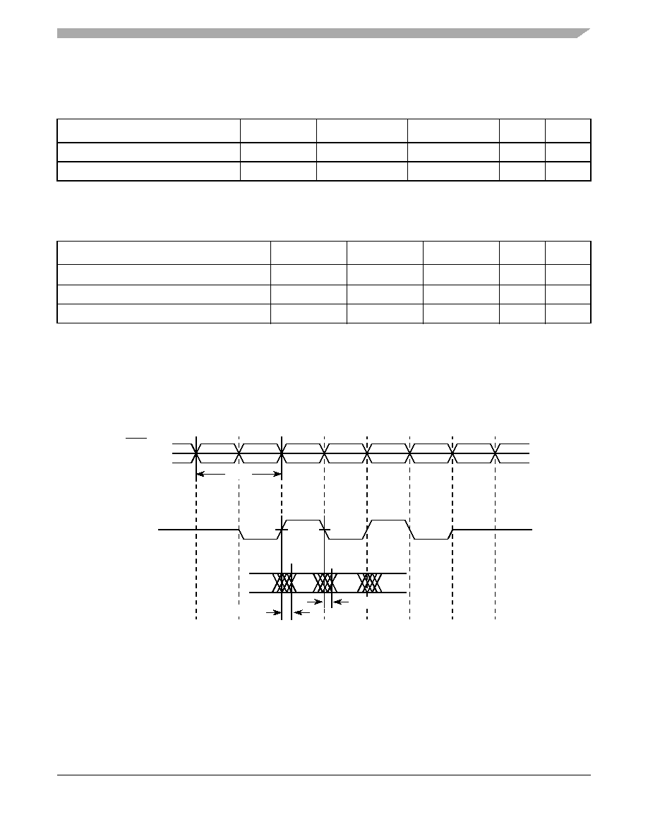
This figure illustrates the DDR input timing diagram showing the tDISKEW timing parameter.
Figure 4. DDR Input Timing Diagram
Table 18. DDR SDRAM Input AC Timing Specifications for 2.5-V Interface
At recommended operating conditions with GVDD of 2.5 ± 5%.
Parameter
Symbol
Min
Max
Unit
Note
AC input low voltage
VIL
—MVREF – 0.31
V
—
AC input high voltage
VIH
MVREF + 0.31
—
V
—
Table 19. DDR and DDR2 SDRAM Input AC Timing Specifications
At recommended operating conditions. with GVDD of 2.5 ± 5%.
Parameter
Symbol
Min
Max
Unit
Note
Controller skew for MDQS—MDQ
tCISKEW
—
ps
1, 2
333 MHz
—
–750
750
—
266 MHz
—
–750
750
—
Notes:
1. tCISKEW represents the total amount of skew consumed by the controller between MDQS[n] and any corresponding bit that
is captured with MDQS[n]. This should be subtracted from the total timing budget.
2. The amount of skew that can be tolerated from MDQS to a corresponding MDQ signal is called tDISKEW. This can be
determined by the following equation: tDISKEW = ± (T/4 – abs(tCISKEW)) where T is the clock period and abs(tCISKEW) is the
absolute value of tCISKEW.
MCK[n]
tMCK
MDQ[x]
MDQS[n]
D1
D0
tDISKEW
相關PDF資料 |
PDF描述 |
|---|---|
| 1-1734798-1 | CONN HOUSING FPC 11POS R/A SMD |
| MPC8313ZQADD | IC MPU POWERQUICC II PRO 516PBGA |
| 3-1734592-1 | CONN FPC 31POS .5MM RT ANG SMD |
| 346-012-526-804 | CARDEDGE 12POS DUAL .125 GREEN |
| 346-012-526-802 | CARDEDGE 12POS DUAL .125 GREEN |
相關代理商/技術(shù)參數(shù) |
參數(shù)描述 |
|---|---|
| MPC8313ZQAFFA | 制造商:FREESCALE 制造商全稱:Freescale Semiconductor, Inc 功能描述:PowerQUICC? II Pro Processor Hardware Specifications |
| MPC8313ZQAFFB | 功能描述:微處理器 - MPU REV2.1 W/OENCR RoHS:否 制造商:Atmel 處理器系列:SAMA5D31 核心:ARM Cortex A5 數(shù)據(jù)總線寬度:32 bit 最大時鐘頻率:536 MHz 程序存儲器大小:32 KB 數(shù)據(jù) RAM 大小:128 KB 接口類型:CAN, Ethernet, LIN, SPI,TWI, UART, USB 工作電源電壓:1.8 V to 3.3 V 最大工作溫度:+ 85 C 安裝風格:SMD/SMT 封裝 / 箱體:FBGA-324 |
| MPC8313ZQAFFC | 功能描述:微處理器 - MPU 8313 REV2.2 PB NO ENC RoHS:否 制造商:Atmel 處理器系列:SAMA5D31 核心:ARM Cortex A5 數(shù)據(jù)總線寬度:32 bit 最大時鐘頻率:536 MHz 程序存儲器大小:32 KB 數(shù)據(jù) RAM 大小:128 KB 接口類型:CAN, Ethernet, LIN, SPI,TWI, UART, USB 工作電源電壓:1.8 V to 3.3 V 最大工作溫度:+ 85 C 安裝風格:SMD/SMT 封裝 / 箱體:FBGA-324 |
| MPC8313ZQAGDC | 功能描述:微處理器 - MPU 8313 REV2.2 PB NO ENC RoHS:否 制造商:Atmel 處理器系列:SAMA5D31 核心:ARM Cortex A5 數(shù)據(jù)總線寬度:32 bit 最大時鐘頻率:536 MHz 程序存儲器大小:32 KB 數(shù)據(jù) RAM 大小:128 KB 接口類型:CAN, Ethernet, LIN, SPI,TWI, UART, USB 工作電源電壓:1.8 V to 3.3 V 最大工作溫度:+ 85 C 安裝風格:SMD/SMT 封裝 / 箱體:FBGA-324 |
| MPC8313ZQGDD | 制造商:FREESCALE 制造商全稱:Freescale Semiconductor, Inc 功能描述:PowerQUICC? II Pro Processor Hardware Specifications |
發(fā)布緊急采購,3分鐘左右您將得到回復。