- 您現(xiàn)在的位置:買賣IC網(wǎng) > PDF目錄371134 > MPC106ARX83CE (MOTOROLA INC) PCI Bridge/Memory Controller PDF資料下載
參數(shù)資料
| 型號(hào): | MPC106ARX83CE |
| 廠商: | MOTOROLA INC |
| 元件分類: | 總線控制器 |
| 英文描述: | PCI Bridge/Memory Controller |
| 中文描述: | PCI BUS CONTROLLER, CBGA304 |
| 封裝: | 21 X 25 MM, 3.16 MM HEIGHT, 1.27 MM PITCH, CERAMIC, BGA-304 |
| 文件頁(yè)數(shù): | 8/28頁(yè) |
| 文件大?。?/td> | 158K |
| 代理商: | MPC106ARX83CE |
第1頁(yè)第2頁(yè)第3頁(yè)第4頁(yè)第5頁(yè)第6頁(yè)第7頁(yè)當(dāng)前第8頁(yè)第9頁(yè)第10頁(yè)第11頁(yè)第12頁(yè)第13頁(yè)第14頁(yè)第15頁(yè)第16頁(yè)第17頁(yè)第18頁(yè)第19頁(yè)第20頁(yè)第21頁(yè)第22頁(yè)第23頁(yè)第24頁(yè)第25頁(yè)第26頁(yè)第27頁(yè)第28頁(yè)
8
MPC106 PCI Bridge/Memory Controller Hardware Specifications
Electrical and Thermal Characteristics
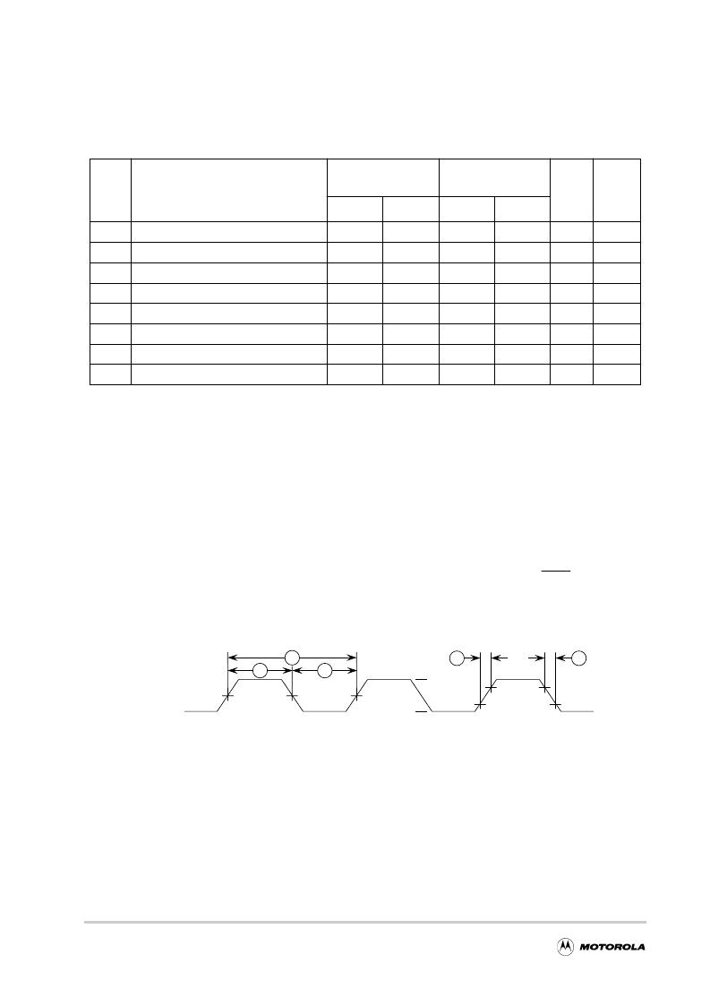
Figure 2 provides the SYSCLK input timing diagram.
Figure 2. SYSCLK Input Timing Diagram
1.4.2.2 Input AC Specifications
Table 7 provides the input AC timing specifications for the 106 as defined in Figure 3 and Figure 4. These
specifications are for operation between 16.67 and 33.33 MHz PCI bus clock (SYSCLK) frequencies.
Assume Vdd = AVdd = 3.3 ± 5% V DC, GND = 0 V DC, and 0
≤
T
j
≤
105 °C.
Table 6. Clock AC Timing Specifications
Num
Characteristic
SYSCLK/Core
33/66 MHz
SYSCLK/Core
33/83.3 MHz
Unit
Notes
Min
Max
Min
Max
—
60x processor bus (core) frequency
16.67
66
16.67
83.3
MHz
1
—
VCO frequency
120
200
120
200
MHz
1, 2
—
SYSCLK frequency
16.67
33.33
16.67
33.33
MHz
1
1
SYSCLK cycle time
30.0
60.0
30.0
60.0
ns
—
2, 3
SYSCLK rise and fall time
—
2.0
—
2.0
ns
3
4
SYSCLK duty cycle measured at 1.4 V
40
60
40
60
%
4
—
SYSCLK jitter
—
±200
—
±200
ps
5
—
106 internal PLL relock time
—
100
—
100
μ
s
4, 6
Notes
1
Caution
frequency, CPU (core) frequency, and PLL (VCO) frequency do not exceed their respective maximum or minimum
operating frequencies. Refer to the PLL[0–3] signal description in Section 1.8, “System Design Information,” for
valid PLL[0–3] settings, and to Section 1.9, “Document Revision History,” for available frequencies and part
numbers.
2
VCO operating range for extended temperature devices is different. Refer to MPC106ARXTGPNS/D for more
information.
3
Rise and fall times for the SYSCLK input are measured from 0.4 V to 2.4 V.
4
Timing is guaranteed by design and characterization and is not tested.
5
The total input jitter (short-term and long-term combined) must be under ±200 ps.
6
PLL-relock time is the maximum time required for PLL lock after a stable Vdd, AVdd, and SYSCLK are reached
during the power-on reset sequence. This specification also applies when the PLL has been disabled and
subsequently re-enabled during the sleep and suspend power-saving modes. Also note that HRST must be held
asserted for a minimum of 255 bus clocks after the PLL-relock time (100
μ
s) during the power-on reset sequence.
:
: The SYSCLK frequency and PLL[0–3] settings must be chosen such that the resulting SYSCLK (bus)
VM
VM = Midpoint Voltage (1.4 V)
2
3
CV
IL
CV
IH
1
SYSCLK
VM
VM
4
4
相關(guān)PDF資料 |
PDF描述 |
|---|---|
| MPC106ARX83CG | PCI Bridge/Memory Controller |
| MPC106ARX83DE | PCI Bridge/Memory Controller |
| MPC106ARX83DG | PCI Bridge/Memory Controller |
| MPC106ARX83TE | PCI Bridge/Memory Controller |
| MPC106ARX83TG | PCI Bridge/Memory Controller |
相關(guān)代理商/技術(shù)參數(shù) |
參數(shù)描述 |
|---|---|
| MPC106ARX83CG | 制造商:MOTOROLA 制造商全稱:Motorola, Inc 功能描述:PCI Bridge/Memory Controller |
| MPC106ARX83DE | 制造商:MOTOROLA 制造商全稱:Motorola, Inc 功能描述:PCI Bridge/Memory Controller |
| MPC106ARX83DG | 制造商:Freescale Semiconductor 功能描述: |
| MPC106ARX83TE | 制造商:MOTOROLA 制造商全稱:Motorola, Inc 功能描述:PCI Bridge/Memory Controller |
| MPC106ARX83TG | 制造商:MOTOROLA 制造商全稱:Motorola, Inc 功能描述:PCI Bridge/Memory Controller |
發(fā)布緊急采購(gòu),3分鐘左右您將得到回復(fù)。