- 您現(xiàn)在的位置:買(mǎi)賣(mài)IC網(wǎng) > PDF目錄371115 > MJF13007 (ON SEMICONDUCTOR) POWER TRANSISTOR PDF資料下載
參數(shù)資料
| 型號(hào): | MJF13007 |
| 廠商: | ON SEMICONDUCTOR |
| 元件分類(lèi): | 功率晶體管 |
| 英文描述: | POWER TRANSISTOR |
| 中文描述: | 8 A, 400 V, NPN, Si, POWER TRANSISTOR, TO-220 |
| 封裝: | PLASTIC, ISOLATED TO-220, 3 PIN |
| 文件頁(yè)數(shù): | 7/10頁(yè) |
| 文件大?。?/td> | 337K |
| 代理商: | MJF13007 |
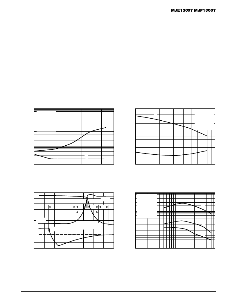
7
Motorola Bipolar Power Transistor Device Data
SWITCHING TIME NOTES
In resistive switching circuits, rise, fall, and storage times
have been defined and apply to both current and voltage
waveforms since they are in phase. However, for inductive
loads which are common to SWITCHMODE power supplies
and any coil driver, current and voltage waveforms are not in
phase. Therefore, separate measurements must be made on
each waveform to determine the total switching time. For this
reason, the following new terms have been defined.
tsv = Voltage Storage Time, 90% IB1 to 10% Vclamp
trv = Voltage Rise Time, 10–90% Vclamp
tfi = Current Fall Time, 90–10% IC
tti = Current Tail, 10–2% IC
tc = Crossover Time, 10% Vclamp to 10% IC
An enlarged portion of the turn–off waveforms is shown in
Figure 13 to aid in the visual identity of these terms. For the
designer, there is minimal switching loss during storage time
and the predominant switching power losses occur during the
crossover interval and can be obtained using the standard
equation from AN222A:
PSWT = 1/2 VCCIC(tc) f
Typical inductive switching times are shown in Figure 14. In
general, trv + tfi
tc. However, at lower test currents this rela-
tionship may not be valid.
As is common with most switching transistors, resistive
switching is specified at 25
°
C and has become a benchmark
for designers. However, for designers of high frequency con-
verter circuits, the user oriented specifications which make
this a “SWITCHMODE” transistor are the inductive switching
speeds (tc and tsv) which are guaranteed at 100
°
C.
SWITCHING PERFORMANCE
1
2
3
4
5
6
7
8 9 10
t
IC, COLLECTOR CURRENT (AMP)
Figure 11. Turn–On Time (Resistive Load)
VCC = 125 V
IC/IB = 5
IB(on) = IB(off)
TJ = 25
°
C
PW = 25
μ
s
t
2
3
4
5
6
7
8
9 10
IC, COLLECTOR CURRENT (AMP)
Figure 12. Turn–Off Time (Resistive Load)
1
t
IC, COLLECTOR CURRENT (AMP)
0.1
0.2
0.3
0.5 0.7
1
2
3
5
7
10
Figure 13. Inductive Switching Measurements
TIME
Figure 14. Typical Inductive Switching Times
10000
1000
100
10
10000
7000
100
200
500
700
1000
2000
5000
10000
10
20
50
100
200
500
1000
2000
5000
VCC = 125 V
IC/IB = 5
IB(on) = IB(off)
TJ = 25
°
C
PW = 25
μ
s
IC/IB = 5
IB(off) = IC/2
Vclamp = 300 V
LC = 200
μ
H
VCC = 15 V
TJ = 25
°
C
ts
tf
td
tr
tc
tfi
tsv
IC
IB
Vclamp
90% IB1
90% Vclamp
90% IC
tfi
Vclamp
10%
Vclamp
10%
IC
2%
IC
tsv
trv
tti
tc
相關(guān)PDF資料 |
PDF描述 |
|---|---|
| MJF13007 | POWER TRANSISTOR 8.0 AMPERES 400 VOLTS 80/40 WATTS |
| MJE13007 | High Voltage Switch Mode Application |
| MJE13007 | TRIPLE DIFFUSED NPN TRANSISTOR (SWITCHING REGULATOR, HIGH VOLTAGE SWITCHING, HIGH SPEED DC-DC CONVERTER) |
| MJE13007 | POWER TRANSISTORS(8A,300-400V,80W) |
| MJE13009 | 12 AMPERE NPN SILICON POWER TRANSISTOR 400 VOLTS 100 WATTS |
相關(guān)代理商/技術(shù)參數(shù) |
參數(shù)描述 |
|---|---|
| MJF13009 | 制造商:ISC 制造商全稱:Inchange Semiconductor Company Limited 功能描述:isc Silicon NPN Power Transistor |
| MJF15030 | 功能描述:兩極晶體管 - BJT 8A 150V 36W NPN RoHS:否 制造商:STMicroelectronics 配置: 晶體管極性:PNP 集電極—基極電壓 VCBO: 集電極—發(fā)射極最大電壓 VCEO:- 40 V 發(fā)射極 - 基極電壓 VEBO:- 6 V 集電極—射極飽和電壓: 最大直流電集電極電流: 增益帶寬產(chǎn)品fT: 直流集電極/Base Gain hfe Min:100 A 最大工作溫度: 安裝風(fēng)格:SMD/SMT 封裝 / 箱體:PowerFLAT 2 x 2 |
| MJF15030_06 | 制造商:ONSEMI 制造商全稱:ON Semiconductor 功能描述:COMPLEMENTARY SILICON POWER TRANSISTORS 8 AMPERES 150 VOLTS, 36 WATTS |
| MJF15030_08 | 制造商:ONSEMI 制造商全稱:ON Semiconductor 功能描述:Complementary Power Transistors |
| MJF15030G | 功能描述:兩極晶體管 - BJT 8A 150V 36W NPN RoHS:否 制造商:STMicroelectronics 配置: 晶體管極性:PNP 集電極—基極電壓 VCBO: 集電極—發(fā)射極最大電壓 VCEO:- 40 V 發(fā)射極 - 基極電壓 VEBO:- 6 V 集電極—射極飽和電壓: 最大直流電集電極電流: 增益帶寬產(chǎn)品fT: 直流集電極/Base Gain hfe Min:100 A 最大工作溫度: 安裝風(fēng)格:SMD/SMT 封裝 / 箱體:PowerFLAT 2 x 2 |
發(fā)布緊急采購(gòu),3分鐘左右您將得到回復(fù)。