- 您現(xiàn)在的位置:買賣IC網(wǎng) > PDF目錄371081 > MCM44D64 (Motorola, Inc.) 1MB R4000 Secondary Cache Fast Static RAM Module Set PDF資料下載
參數(shù)資料
| 型號: | MCM44D64 |
| 廠商: | Motorola, Inc. |
| 英文描述: | 1MB R4000 Secondary Cache Fast Static RAM Module Set |
| 中文描述: | 1MB的二級高速緩存R4000的快速靜態(tài)存儲器模塊集 |
| 文件頁數(shù): | 3/8頁 |
| 文件大小: | 103K |
| 代理商: | MCM44D64 |
MCM4464 SERIES
3
MOTOROLA FAST SRAM
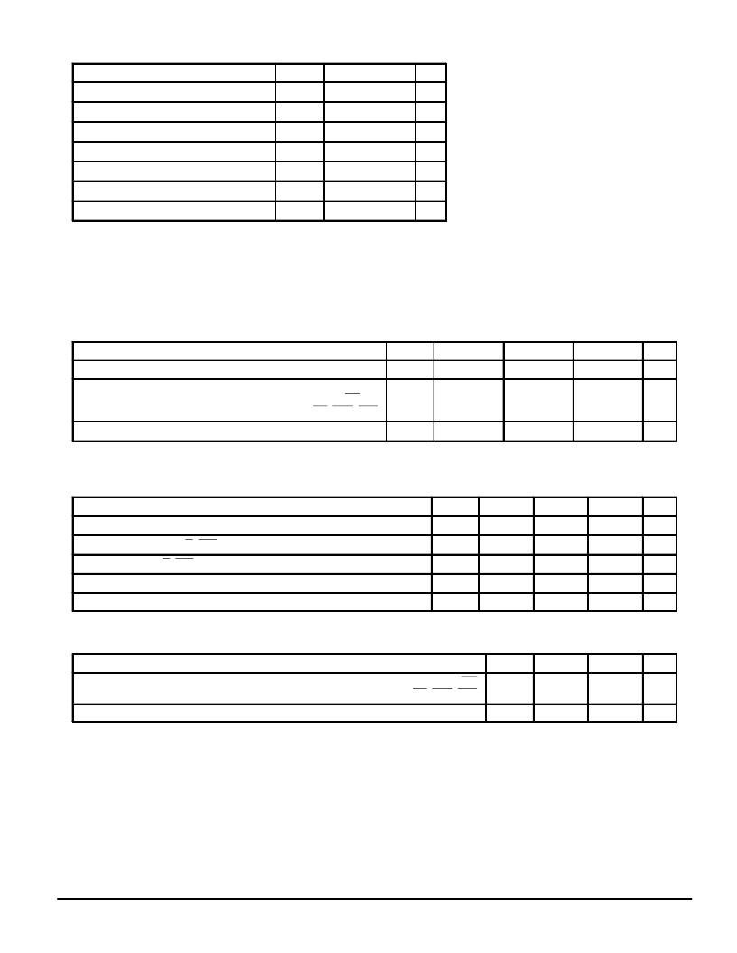
ABSOLUTE MAXIMUM RATINGS
(Voltages Referenced to VSS = 0 V)
Rating
Symbol
Value
Unit
Power Supply Voltage
VCC
– 0.5 to 7.0
V
Voltage Relative to VSS
Vin, Vout
– 0.5 to VCC + 0.5
V
Output Current (per I/O)
Iout
±
30
mA
Power Dissipation
PD
10
W
Temperature Under Bias
Tbias
– 10 to + 85
°
C
Operating Temperature
TA
0 to + 70
°
C
Storage Temperature
Tstg
– 25 to +125
°
C
NOTE: Permanent device damage may occur if ABSOLUTE MAXIMUM RATINGS are
exceeded. Functional operation should be restricted to RECOMMENDED OPER-
ATING CONDITIONS. Exposure to higher than recommended voltages for
extended periods of time could affect device reliability.
DC OPERATING CONDITIONS AND CHARACTERISTICS
(VCC = 5.0 V
±
10%, TA = 0 to + 70
°
C, Unless Otherwise Noted)
RECOMMENDED OPERATING CONDITIONS
(Voltages referenced to VSS = 0 V)
Parameter
Symbol
Min
Typ
Max
Unit
Supply Voltage (Operating Voltage Range)
VCC
VIH
4.5
5.0
5.5
V
Input High Voltage
(DQ0 – 35, TDQ0 – 7, WE, A0)
(A1 – A15, OE, DCS, TCS)
2.2
2.0
—
—
VCC + 0.3 V*
VCC + 0.3 V*
V
Input Low Voltage
VIL
– 0.5
**
—
0.8
V
*VIH (max) = VCC + 0.3 V dc; VIH (max) = VCC + 2 V ac (pulse width
≤
20 ns)
**VIL (min) = – 3.0 V ac (pulse width
≤
20 ns)
DC CHARACTERISTICS
Parameter
Symbol
Min
Typ
Max
Unit
Input Leakage Current (All Inputs, Vin = 0 to VCC)
Ilkg(I)
±
10
μ
A
Output Leakage Current (G, xCS = VIH, Vout = 0 to VCC)
Ilkg(O)
±
10
μ
A
AC Supply Current (G, xCS = VIL, Iout = 0 mA)
ICCA
1850
mA
Output Low Voltage (IOL = + 8 mA)
VOL
0.4
V
OUtput High Voltage (IOH = – 4.0 mA)
Note: Good decoupling of the local power supply should always be used.
VOH
2.4
V
CAPACITANCE
(f = 1.0 MHz, dV = 3.0 V, TA = 25
°
C, Periodically Sampled Rather Than 100% Tested)
Parameter
Symbol
Typ
Max
Unit
Input Capacitance
(A0, WE)
(A1 – A15, OE, DCS, TCS)
Cin
Cin
110
10
pF
pF
Input/Output Capacitance
Cout
10
pF
This devices on this module contain circuitry
to protect the inputs against damage due to
high static voltages or electric fields; however,
it is advised that normal precautions be taken
to avoid application of any voltage higher than
maximum rated voltages to these high–imped-
ance circuits.
These BiCMOS memory circuits have been
designed to meet the dc and ac specifications
shown in the tables, after thermal equilibrium
has been established. The module is in a test
socket or mounted on a printed circuit board
and transverse air flow of at leat 500 linear feet
per minute is maintained.
相關(guān)PDF資料 |
PDF描述 |
|---|---|
| MCM44E64 | 1MB R4000 Secondary Cache Fast Static RAM Module Set |
| MCM44F64 | 1MB R4000 Secondary Cache Fast Static RAM Module Set |
| MCM44C256B | 4MB R4000 Secondary Cache Fast Static RAM Module Set |
| MCM44A256B | FILTER SAW 479.5MHZ |
| MCM44256B | 4MB R4000 Secondary Cache Fast Static RAM Module Set |
相關(guān)代理商/技術(shù)參數(shù) |
參數(shù)描述 |
|---|---|
| MCM44E64 | 制造商:MOTOROLA 制造商全稱:Motorola, Inc 功能描述:1MB R4000 Secondary Cache Fast Static RAM Module Set |
| MCM44F64 | 制造商:MOTOROLA 制造商全稱:Motorola, Inc 功能描述:1MB R4000 Secondary Cache Fast Static RAM Module Set |
| MCM44G64 | 制造商:MOTOROLA 制造商全稱:Motorola, Inc 功能描述:1MB R4000 Secondary Cache Fast Static RAM Module Set |
| MCM44H64 | 制造商:MOTOROLA 制造商全稱:Motorola, Inc 功能描述:1MB R4000 Secondary Cache Fast Static RAM Module Set |
| MCM4517P12 | 制造商:Motorola Inc 功能描述: |
發(fā)布緊急采購,3分鐘左右您將得到回復(fù)。