- 您現(xiàn)在的位置:買賣IC網(wǎng) > PDF目錄371081 > MCM44D64 (Motorola, Inc.) 1MB R4000 Secondary Cache Fast Static RAM Module Set PDF資料下載
參數(shù)資料
| 型號: | MCM44D64 |
| 廠商: | Motorola, Inc. |
| 英文描述: | 1MB R4000 Secondary Cache Fast Static RAM Module Set |
| 中文描述: | 1MB的二級高速緩存R4000的快速靜態(tài)存儲器模塊集 |
| 文件頁數(shù): | 1/8頁 |
| 文件大小: | 103K |
| 代理商: | MCM44D64 |
MCM4464 SERIES
1
Motorola, Inc. 1994
1MB R4000 Secondary Cache
Fast Static RAM Module Set
Four MCM4464 modules comprise a full 1 MB of secondary cache for the
R4000 processor. Each module contains nine MCM6709J fast static RAMs for
a cache data size of 64K x 36. The tag portion, dependent on word line size,
contains either two MCM6709J or one MCM6706J fast static RAMs. All input sig-
nals, except A0 and WE are buffered using 74FBT2827 drivers with series 25
resistors.
The MCM6709J and MCM6706J are fabricated using high–performance sili-
con–gate BiCMOS technology. Static design eliminates the need for internal
clocks or timing strobes.
All 1MB R4000 supported secondary cache options are available.
Single 5 V
±
10% Power Supply
All Inputs and Outputs are TTL Compatible
Three State Outputs
Fast Module Access Time: 12/15/17 ns
Zero Wait–State Operation
Unified or Split Seconday Cache Modules are Available (See Ordering
Information for Details)
Word Line Sizes of 4, 8, 16, and 32 are Available (See Ordering
Information for Details)
The Pin Compatible MCM44256 Series is also Available to Support a Full
4MB R4000 Secondary Cache.
Decoupling Capacitors are Used for Each Fast Static RAM and Buffer,
Along with Bulk Capacitance for Maximum Noise Immunity
High Quality Multi–Layer FR4 PWB with Separate Power and Ground
Planes
PIN NAMES
A0 – A15
WE
. . . . . . . . . . . . . . . . . . . . . . .
DCS
. . . . . . . . . . . . . . . . . . . . . .
TCS
. . . . . . . . . . . . . . . . . . . . . . .
OE
. . . . . . . . . . . . . . . . . . . . .
DQ0 – DQ35
. . . . . . . . .
TDQ0 – TDQ7
. . .
VCC
. . . . . . . . . . . . . . . .
VSS
. . . . . . . . . . . . . . . . . . . . . . . . . .
Address Inputs
Write Enable
Data Enable
Tag Enable
Output Enable
Data Input / Output
TAG Data Input / Output
+ 5 V Power Supply
. . . . . . . . . . . . . . . .
Ground
For proper operation of the device, VSS must
be connected to ground.
Order this document
by MCM4464/D
SEMICONDUCTOR TECHNICAL DATA
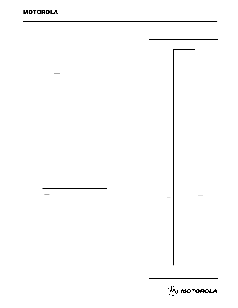
PIN ASSIGNMENT
80 LEAD SIMM — TOP VIEW
MCM4464 Series
VCC
DQ1
2
4
6
DQ5
VSS
DQ8
DQ10
DQ12
DQ14
DQ15
DQ17
DQ19
DQ21
VSS
DQ23
DQ25
DQ27
DQ29
VSS
DQ0
DQ2
DQ4
DQ6
DQ9
DQ11
DQ13
VSS
DQ16
DQ18
DQ20
DQ22
VCC
DQ24
DQ28
DQ7
19
21
23
25
27
29
1
3
5
7
9
11
13
15
17
20
22
24
26
28
30
32
8
10
12
14
16
18
31
DQ3
33
35
37
39
34
36
38
40
DQ31
VSS
DQ26
DQ34
VSS
42
44
A0
A2
A4
A6
VCC
OE
A8
A10
VSS
A13
A15
NC
TDQ0
TDQ1
TDQ3
DQ33
DQ35
WE
A1
A3
VSS
DCS
A7
A9
A11
A12
A14
NC
TCS
TDQ4
A5
59
61
63
65
67
69
41
43
45
47
49
51
53
55
57
60
62
64
66*
68*
70
72
74
46
48
50
52
54
56
58
71
73
75
77
76
78
80
79
VCC
TDQ6
TDQ2
VSS
DQ30
DQ32
TDQ5
TDQ7
VSS
NOTE: Pin assignment is for unified cache. For
split cache option, Pin 68 becomes
Address MSB (A15) and Pin 66 is NC.
REV 1
8/94
相關PDF資料 |
PDF描述 |
|---|---|
| MCM44E64 | 1MB R4000 Secondary Cache Fast Static RAM Module Set |
| MCM44F64 | 1MB R4000 Secondary Cache Fast Static RAM Module Set |
| MCM44C256B | 4MB R4000 Secondary Cache Fast Static RAM Module Set |
| MCM44A256B | FILTER SAW 479.5MHZ |
| MCM44256B | 4MB R4000 Secondary Cache Fast Static RAM Module Set |
相關代理商/技術參數(shù) |
參數(shù)描述 |
|---|---|
| MCM44E64 | 制造商:MOTOROLA 制造商全稱:Motorola, Inc 功能描述:1MB R4000 Secondary Cache Fast Static RAM Module Set |
| MCM44F64 | 制造商:MOTOROLA 制造商全稱:Motorola, Inc 功能描述:1MB R4000 Secondary Cache Fast Static RAM Module Set |
| MCM44G64 | 制造商:MOTOROLA 制造商全稱:Motorola, Inc 功能描述:1MB R4000 Secondary Cache Fast Static RAM Module Set |
| MCM44H64 | 制造商:MOTOROLA 制造商全稱:Motorola, Inc 功能描述:1MB R4000 Secondary Cache Fast Static RAM Module Set |
| MCM4517P12 | 制造商:Motorola Inc 功能描述: |
發(fā)布緊急采購,3分鐘左右您將得到回復。