- 您現(xiàn)在的位置:買賣IC網(wǎng) > PDF目錄359153 > MCF52235 (飛思卡爾半導(dǎo)體(中國)有限公司) ColdFire Microcontroller PDF資料下載
參數(shù)資料
| 型號: | MCF52235 |
| 廠商: | 飛思卡爾半導(dǎo)體(中國)有限公司 |
| 英文描述: | ColdFire Microcontroller |
| 中文描述: | ColdFire微控制器 |
| 文件頁數(shù): | 32/50頁 |
| 文件大?。?/td> | 656K |
| 代理商: | MCF52235 |
第1頁第2頁第3頁第4頁第5頁第6頁第7頁第8頁第9頁第10頁第11頁第12頁第13頁第14頁第15頁第16頁第17頁第18頁第19頁第20頁第21頁第22頁第23頁第24頁第25頁第26頁第27頁第28頁第29頁第30頁第31頁當(dāng)前第32頁第33頁第34頁第35頁第36頁第37頁第38頁第39頁第40頁第41頁第42頁第43頁第44頁第45頁第46頁第47頁第48頁第49頁第50頁
MCF52235 ColdFire Microcontroller, Rev. 3
Preliminary Electrical Characteristics
Freescale Semiconductor
32
2.3
DC Electrical Specifications
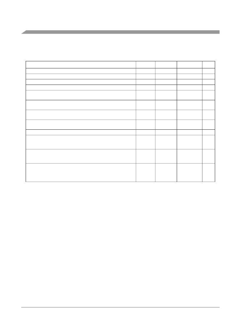
Table 22. DC Electrical Specifications
1
1
Refer to
Table 25
for additional PLL specifications.
2
Refer to
Table 3
for pins with internal pull-up devices.
3
This parameter is characterized before qualification rather than 100% tested.
4
pF load ratings are based on DC loading and are provided as an indication of driver strength. High speed interfaces
require transmission line analysis to determine proper drive strength and termination.
5
All functional non-supply pins are internally clamped to V
SS
and their respective V
DD
.
6
Input must be current limited to the value specified. To determine the value of the required current-limiting resistor,
calculate resistance values for positive and negative clamp voltages, then use the larger of the two values.
7
The power supply must maintain regulation within operating V
DD
range during instantaneous and operating maximum
current conditions. If positive injection current (V
in
> V
DD
) is greater than I
DD
, the injection current may flow out of V
DD
and could result in external power supply going out of regulation. Ensure that the external V
DD
load will shunt current
greater than maximum injection current. This will be the greatest risk when the MCU is not consuming power. Examples
are: if no system clock is present, or if clock rate is very low which would reduce overall power consumption. Also, the
system clock is not present during the power-up sequence until the PLL has attained lock.
Characteristic
Symbol
Min
Max
Unit
Supply voltage
Input high voltage
Input low voltage
Input hysteresis
Input leakage current
V
in
= V
DD
or V
SS
, input-only pins
High impedance (off-state) leakage current
V
in
= V
DD
or V
SS
, all input/output and output pins
Output high voltage (all input/output and all output pins)
I
OH
= –2.0 mA
Output low voltage (all input/output and all output pins)
I
OL
= 2.0 mA
Weak internal pull-up device current, tested at V
IL
max.
2
Input capacitance
3
All input-only pins
All input/output (three-state) pins
Load capacitance
4
Low drive strength
High drive strength
DC injection current
3,
5, 6, 7
V
NEGCLAMP
=V
SS
– 0.3 V, V
POSCLAMP
= V
DD
+ 0.3
Single pin limit
Total MCU limit, Includes sum of all stressed pins
V
DD
V
IH
V
IL
V
HYS
I
in
3.0
3.6
4.0
V
V
V
0.7
×
V
DD
V
SS
– 0.3
0.06
×
V
DD
–1.0
0.35 x V
DD
—
1.0
mV
μ
A
I
OZ
–1.0
1.0
μ
A
V
OH
V
DD
- 0.5
__
V
V
OL
__
0.5
V
I
APU
C
in
–10
–130
μ
A
pF
—
—
7
7
C
L
25
50
pF
I
IC
–1.0
–10
1.0
10
mA
相關(guān)PDF資料 |
PDF描述 |
|---|---|
| MCF5232CAB80 | Integrated Microprocessor Hardware Specification |
| MCF5232 | Integrated Microprocessor Hardware Specification |
| MCF5249 | CodeWarrior Development Studio for ColdFire㈢ Architectures |
| MCF5251_07 | ColdFire㈢ Microprocessor Data Sheet |
| MCF5251 | ColdFire Processor |
相關(guān)代理商/技術(shù)參數(shù) |
參數(shù)描述 |
|---|---|
| MCF52235_06 | 制造商:FREESCALE 制造商全稱:Freescale Semiconductor, Inc 功能描述:ColdFire㈢ Microcontroller |
| MCF52235_07 | 制造商:FREESCALE 制造商全稱:Freescale Semiconductor, Inc 功能描述:Microcontroller |
| MCF52235_10 | 制造商:FREESCALE 制造商全稱:Freescale Semiconductor, Inc 功能描述:MCF52235 ColdFire Microcontroller Data Sheet |
| MCF52235CAL60 | 功能描述:32位微控制器 - MCU KIRIN2E EPP RoHS:否 制造商:Texas Instruments 核心:C28x 處理器系列:TMS320F28x 數(shù)據(jù)總線寬度:32 bit 最大時鐘頻率:90 MHz 程序存儲器大小:64 KB 數(shù)據(jù) RAM 大小:26 KB 片上 ADC:Yes 工作電源電壓:2.97 V to 3.63 V 工作溫度范圍:- 40 C to + 105 C 封裝 / 箱體:LQFP-80 安裝風(fēng)格:SMD/SMT |
| MCF52235CAL60A | 制造商:Freescale Semiconductor 功能描述:KIRIN2E EPP - REV A - Bulk |
發(fā)布緊急采購,3分鐘左右您將得到回復(fù)。