- 您現(xiàn)在的位置:買賣IC網(wǎng) > PDF目錄359660 > MC9S12DJ128B (飛思卡爾半導體(中國)有限公司) Device User Guide V01.09 PDF資料下載
參數(shù)資料
| 型號: | MC9S12DJ128B |
| 廠商: | 飛思卡爾半導體(中國)有限公司 |
| 英文描述: | Device User Guide V01.09 |
| 中文描述: | 設(shè)備的用戶手冊V01.09 |
| 文件頁數(shù): | 89/128頁 |
| 文件大小: | 729K |
| 代理商: | MC9S12DJ128B |
第1頁第2頁第3頁第4頁第5頁第6頁第7頁第8頁第9頁第10頁第11頁第12頁第13頁第14頁第15頁第16頁第17頁第18頁第19頁第20頁第21頁第22頁第23頁第24頁第25頁第26頁第27頁第28頁第29頁第30頁第31頁第32頁第33頁第34頁第35頁第36頁第37頁第38頁第39頁第40頁第41頁第42頁第43頁第44頁第45頁第46頁第47頁第48頁第49頁第50頁第51頁第52頁第53頁第54頁第55頁第56頁第57頁第58頁第59頁第60頁第61頁第62頁第63頁第64頁第65頁第66頁第67頁第68頁第69頁第70頁第71頁第72頁第73頁第74頁第75頁第76頁第77頁第78頁第79頁第80頁第81頁第82頁第83頁第84頁第85頁第86頁第87頁第88頁當前第89頁第90頁第91頁第92頁第93頁第94頁第95頁第96頁第97頁第98頁第99頁第100頁第101頁第102頁第103頁第104頁第105頁第106頁第107頁第108頁第109頁第110頁第111頁第112頁第113頁第114頁第115頁第116頁第117頁第118頁第119頁第120頁第121頁第122頁第123頁第124頁第125頁第126頁第127頁第128頁
A.1.5 Absolute Maximum Ratings
Absolute maximum ratings are stress ratings only. A functional operation under or outside those maxima
is not guaranteed. Stress beyond those limits may affect the reliability or cause permanent damage of the
device.
This device contains circuitry protecting against damage due to high static voltage or electrical fields;
however, it is advised that normal precautions be taken to avoid application of any voltages higher than
maximum-rated voltages to this high-impedance circuit. Reliability of operation is enhanced if unused
inputs are tied to an appropriate logic voltage level (e.g., either V
SS5
or V
DD5
).
A.1.6 ESD Protection and Latch-up Immunity
All ESD testing is in conformity with CDF-AEC-Q100 Stress test qualification for Automotive Grade
Integrated Circuits. During the device qualification ESD stresses were performed for the Human Body
Model (HBM), the Machine Model (MM) and the Charge Device Model.
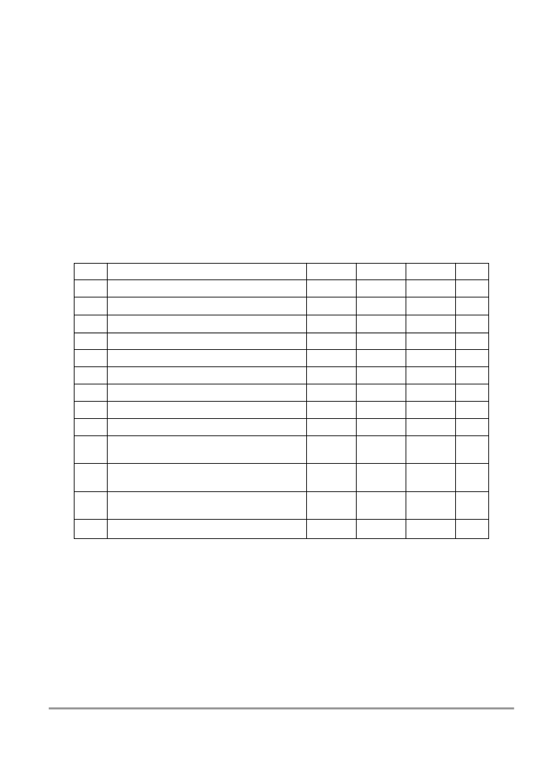
Table A-1 Absolute Maximum Ratings
1
NOTES
:
1. Beyond absolute maximum ratings device might be damaged.
2. The device contains an internal voltage regulator to generate the logic and PLL supply out of the I/O supply.
The absolute maximum ratings apply when the device is powered from an external source.
3. All digital I/O pins are internally clamped to V
SSX
and V
DDX
, V
SSR
and V
DDR
or V
SSA
and V
DDA
.
4. Those pins are internally clamped to V
SSPLL
and V
DDPLL
.
5. This pin is clamped low to V
SSPLL
, but not clamped high. This pin must be tied low in applications.
Num
Rating
Symbol
Min
Max
Unit
1
I/O, Regulator and Analog Supply Voltage
V
DD5
-0.3
6.0
V
2
Digital Logic Supply Voltage
2
V
DD
-0.3
3.0
V
3
PLL Supply Voltage
2
V
DDPLL
-0.3
3.0
V
4
Voltage difference VDDX to VDDR and VDDA
VDDX
-0.3
0.3
V
5
Voltage difference VSSX to VSSR and VSSA
VSSX
-0.3
0.3
V
6
Digital I/O Input Voltage
V
IN
-0.3
6.0
V
7
Analog Reference
V
RH,
V
RL
-0.3
6.0
V
8
XFC, EXTAL, XTAL inputs
V
ILV
-0.3
3.0
V
9
TEST input
V
TEST
-0.3
10.0
V
10
Instantaneous Maximum Current
Single pin limit for all digital I/O pins
3
I
D
-25
+25
mA
11
Instantaneous Maximum Current
Single pin limit for XFC, EXTAL, XTAL
4
I
DL
-25
+25
mA
12
Instantaneous Maximum Current
Single pin limit for TEST
5
I
DT
-0.25
0
mA
13
Storage Temperature Range
T
stg
– 65
155
°
C
F
Freescale Semiconductor, Inc.
For More Information On This Product,
Go to: www.freescale.com
n
.
相關(guān)PDF資料 |
PDF描述 |
|---|---|
| MC9S12DT128B | Device User Guide V01.09 |
| MCF5206E | CodeWarrior Development Studio for ColdFire㈢ Architectures |
| mcf5207 | CodeWarrior Development Studio for ColdFire㈢ Architectures |
| MCF5214 | CodeWarrior Development Studio for ColdFire㈢ Architectures |
| MCF5216 | CodeWarrior Development Studio for ColdFire㈢ Architectures |
相關(guān)代理商/技術(shù)參數(shù) |
參數(shù)描述 |
|---|---|
| MC9S12DJ128BCFU | 功能描述:16位微控制器 - MCU 16 Bit 25MHz RoHS:否 制造商:Texas Instruments 核心:RISC 處理器系列:MSP430FR572x 數(shù)據(jù)總線寬度:16 bit 最大時鐘頻率:24 MHz 程序存儲器大小:8 KB 數(shù)據(jù) RAM 大小:1 KB 片上 ADC:Yes 工作電源電壓:2 V to 3.6 V 工作溫度范圍:- 40 C to + 85 C 封裝 / 箱體:VQFN-40 安裝風格:SMD/SMT |
| MC9S12DJ128BCPV | 功能描述:16位微控制器 - MCU 16 Bit 25MHz RoHS:否 制造商:Texas Instruments 核心:RISC 處理器系列:MSP430FR572x 數(shù)據(jù)總線寬度:16 bit 最大時鐘頻率:24 MHz 程序存儲器大小:8 KB 數(shù)據(jù) RAM 大小:1 KB 片上 ADC:Yes 工作電源電壓:2 V to 3.6 V 工作溫度范圍:- 40 C to + 85 C 封裝 / 箱體:VQFN-40 安裝風格:SMD/SMT |
| MC9S12DJ128BMPV | 功能描述:16位微控制器 - MCU 16 Bit 25MHz RoHS:否 制造商:Texas Instruments 核心:RISC 處理器系列:MSP430FR572x 數(shù)據(jù)總線寬度:16 bit 最大時鐘頻率:24 MHz 程序存儲器大小:8 KB 數(shù)據(jù) RAM 大小:1 KB 片上 ADC:Yes 工作電源電壓:2 V to 3.6 V 工作溫度范圍:- 40 C to + 85 C 封裝 / 箱體:VQFN-40 安裝風格:SMD/SMT |
| MC9S12DJ128BVPV | 制造商:Rochester Electronics LLC 功能描述:- Bulk 制造商:Freescale Semiconductor 功能描述: |
| MC9S12DJ128CFU | 制造商:Rochester Electronics LLC 功能描述:128K FLASH HCS12 MCU - Bulk |
發(fā)布緊急采購,3分鐘左右您將得到回復(fù)。