- 您現(xiàn)在的位置:買(mǎi)賣(mài)IC網(wǎng) > PDF目錄224200 > MC9328MXL15 (MOTOROLA INC) 32-BIT, 150 MHz, MICROPROCESSOR, PBGA256 PDF資料下載
參數(shù)資料
| 型號(hào): | MC9328MXL15 |
| 廠(chǎng)商: | MOTOROLA INC |
| 元件分類(lèi): | 微控制器/微處理器 |
| 英文描述: | 32-BIT, 150 MHz, MICROPROCESSOR, PBGA256 |
| 封裝: | 14 X 14 MM, 1.30 MM HEIGHT, 0.80 MM PITCH, MAPBGA-256 |
| 文件頁(yè)數(shù): | 75/84頁(yè) |
| 文件大小: | 1492K |
| 代理商: | MC9328MXL15 |
第1頁(yè)第2頁(yè)第3頁(yè)第4頁(yè)第5頁(yè)第6頁(yè)第7頁(yè)第8頁(yè)第9頁(yè)第10頁(yè)第11頁(yè)第12頁(yè)第13頁(yè)第14頁(yè)第15頁(yè)第16頁(yè)第17頁(yè)第18頁(yè)第19頁(yè)第20頁(yè)第21頁(yè)第22頁(yè)第23頁(yè)第24頁(yè)第25頁(yè)第26頁(yè)第27頁(yè)第28頁(yè)第29頁(yè)第30頁(yè)第31頁(yè)第32頁(yè)第33頁(yè)第34頁(yè)第35頁(yè)第36頁(yè)第37頁(yè)第38頁(yè)第39頁(yè)第40頁(yè)第41頁(yè)第42頁(yè)第43頁(yè)第44頁(yè)第45頁(yè)第46頁(yè)第47頁(yè)第48頁(yè)第49頁(yè)第50頁(yè)第51頁(yè)第52頁(yè)第53頁(yè)第54頁(yè)第55頁(yè)第56頁(yè)第57頁(yè)第58頁(yè)第59頁(yè)第60頁(yè)第61頁(yè)第62頁(yè)第63頁(yè)第64頁(yè)第65頁(yè)第66頁(yè)第67頁(yè)第68頁(yè)第69頁(yè)第70頁(yè)第71頁(yè)第72頁(yè)第73頁(yè)第74頁(yè)當(dāng)前第75頁(yè)第76頁(yè)第77頁(yè)第78頁(yè)第79頁(yè)第80頁(yè)第81頁(yè)第82頁(yè)第83頁(yè)第84頁(yè)
Specifications
MOTOROLA
MC9328MXL Advance Information
77
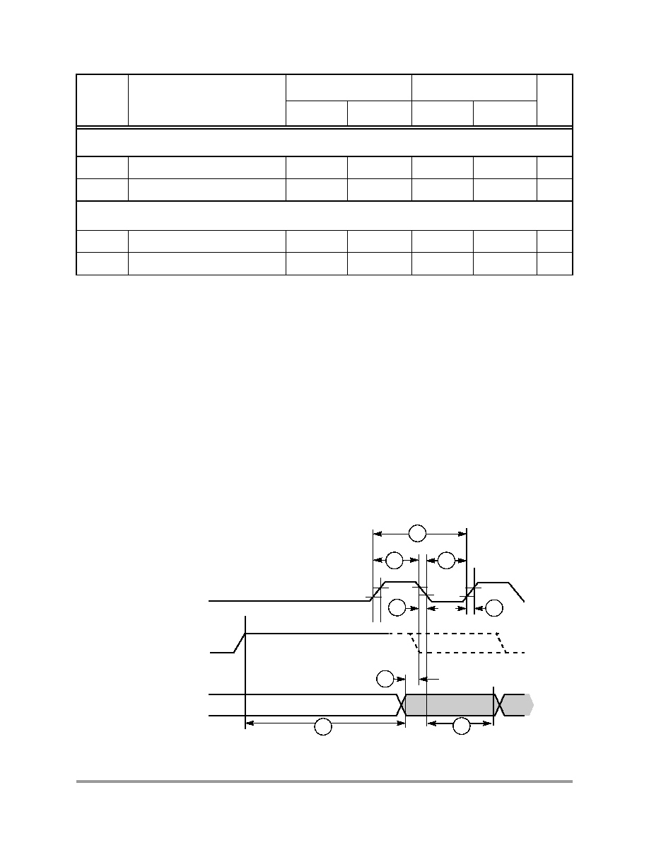
3.18 CMOS Sensor Interface
The CSI module consists of a control register to configure the interface timing, a control register for
statistic data generation, a status register, interface logic, a 32
× 32 image data receive FIFO, and a 16 × 32
statistic data FIFO. Figure 64 shows the timing diagram when the CMOS sensor output data is configured
for negative edge and the CSI is programmed to received data in positive edge. The parameters for the
timing diagram are listed in Table 29 on page 78.
Figure 64. CSI Signal Timing Diagram
Synchronous Internal Clock Operation (Port B Alternate Function2)
31
SRXD setup before STCK falling
18.81
—
16.5
—
ns
32
SRXD hold after STCK falling
0
—
0—
ns
Synchronous External Clock Operation (Port B Alternate Function2)
33
SRXD setup before STCK falling
1.14
—
1.0
—
ns
34
SRXD hold after STCK falling
0
—
0—
ns
1.
All the timings for the SSI are given for a non-inverted serial clock polarity (TSCKP/RSCKP = 0) and a
non-inverted frame sync (TFSI/RFSI = 0). If the polarity of the clock and/or the frame sync have been
inverted, all the timing remains valid by inverting the clock signal STCK/SRCK and/or the frame sync
STFS/SRFS shown in the tables and in the figures.
2.
There are 2 set of I/O signals for the SSI module. They are from Port C primary function (pad 257 to pad
261) and Port B alternate function (pad 283 to pad 288). When SSI signals are configured as outputs, they
can be viewed both at Port C primary function and Port B alternate function. When SSI signals are
configured as inputs, the SSI module selects the input based on FMCR register bits in the Clock controller
module (CRM). By default, the input are selected from Port C primary function.
3.
bl = bit length; wl = word length.
Table 28. SSI (Port B Alternate Function) Timing Parameter Table (Continued)
Ref No.
Parameter
1.8V ± 0.10V
3.0V ± 0.30V
Unit
Minimum
Maximum
Minimum
Maximum
csi_pixclk
4b
4a
3a
2a
1
csi_hsync/csi_d
3b
2b
csi_vsync
valid_data
5
相關(guān)PDF資料 |
PDF描述 |
|---|---|
| MC9328MXL20 | 32-BIT, 200 MHz, MICROPROCESSOR, PBGA256 |
| MCA2231-SM | 1 CHANNEL DARLINGTON OUTPUT OPTOCOUPLER |
| MCA255-X007T | 1 CHANNEL DARLINGTON OUTPUT OPTOCOUPLER |
| MCA255-X017T | 1 CHANNEL DARLINGTON OUTPUT OPTOCOUPLER |
| MCA255-X019T | 1 CHANNEL DARLINGTON OUTPUT OPTOCOUPLER |
相關(guān)代理商/技術(shù)參數(shù) |
參數(shù)描述 |
|---|---|
| MC9328MXLCVF15 | 制造商:FREESCALE 制造商全稱(chēng):Freescale Semiconductor, Inc 功能描述:i.MX Integrated Portable System Processor |
| MC9328MXLCVH15 | 制造商:FREESCALE 制造商全稱(chēng):Freescale Semiconductor, Inc 功能描述:i.MX Integrated Portable System Processor |
| MC9328MXLCVM15 | 功能描述:處理器 - 專(zhuān)門(mén)應(yīng)用 DRAGONBALL CORSICA PB-FR RoHS:否 制造商:Freescale Semiconductor 類(lèi)型:Multimedia Applications 核心:ARM Cortex A9 處理器系列:i.MX6 數(shù)據(jù)總線(xiàn)寬度:32 bit 最大時(shí)鐘頻率:1 GHz 指令/數(shù)據(jù)緩存: 數(shù)據(jù) RAM 大小:128 KB 數(shù)據(jù) ROM 大小: 工作電源電壓: 最大工作溫度:+ 95 C 安裝風(fēng)格:SMD/SMT 封裝 / 箱體:MAPBGA-432 |
| MC9328MXLCVM15 | 制造商:Freescale Semiconductor 功能描述:Microprocessor |
| MC9328MXLCVM15R2 | 功能描述:處理器 - 專(zhuān)門(mén)應(yīng)用 DRAGONBALL CORSICA PB-FR RoHS:否 制造商:Freescale Semiconductor 類(lèi)型:Multimedia Applications 核心:ARM Cortex A9 處理器系列:i.MX6 數(shù)據(jù)總線(xiàn)寬度:32 bit 最大時(shí)鐘頻率:1 GHz 指令/數(shù)據(jù)緩存: 數(shù)據(jù) RAM 大小:128 KB 數(shù)據(jù) ROM 大小: 工作電源電壓: 最大工作溫度:+ 95 C 安裝風(fēng)格:SMD/SMT 封裝 / 箱體:MAPBGA-432 |
發(fā)布緊急采購(gòu),3分鐘左右您將得到回復(fù)。