- 您現(xiàn)在的位置:買(mǎi)賣(mài)IC網(wǎng) > PDF目錄371063 > MC74HC195N (MOTOROLA INC) 4-Bit Universal Shift Register PDF資料下載
參數(shù)資料
| 型號(hào): | MC74HC195N |
| 廠(chǎng)商: | MOTOROLA INC |
| 元件分類(lèi): | 通用總線(xiàn)功能 |
| 英文描述: | 4-Bit Universal Shift Register |
| 中文描述: | HC/UH SERIES, 4-BIT RIGHT PARALLEL IN PARALLEL OUT SHIFT REGISTER, TRUE OUTPUT, PDIP16 |
| 封裝: | PLASTIC, DIP-16 |
| 文件頁(yè)數(shù): | 4/7頁(yè) |
| 文件大小: | 203K |
| 代理商: | MC74HC195N |
MC74HC195
MOTOROLA
High–Speed CMOS Logic Data
DL129 — Rev 6
3–4
PIN DESCRIPTION
DATA INPUTS
A, B, C, D (Pins 4, 5, 6, 7)
Parallel data inputs.
OUTPUTS
QA, QB, QC, QD, QD (Pins 15, 14, 13, 12, 11)
Parallel data outputs.
CONTROL INPUTS
Clock (Pin 10)
Clock input. The shift register is completely static, allowing
Clock rates down to DC in a continuous or intermittent mode.
Serial Shift/Parallel Load (Pin 9)
Shift or load control. A low level applied to this pin allows
data to be loaded from the parallel inputs. Data is loaded with
the positive transition of the Clock input. A high level allows
data to be shifted in the manner dictated by the J and K con-
trol inputs.
Reset (Pin 1)
A low level applied to this pin resets all stages and forces
all outputs low.
J, K (Pins 2, 3)
Shift Control. With Serial Shift/Parallel Load high, J and K
control the mode of operation, as illustrated in the Function
Table.
J = L, K = H
With a positive transition of the Clock input, each bit is
shifted to the right (in the direction QA toward QD) one stage
and stage A maintains its previous state.
J = H, K = L
With a positive transition of the Clock input, each bit is
shifted right (in the direction of QA toward QD) one stage and
the QA output is inverted.
J = K = L
With a positive transition of the Clock input, each bit is
shifted right (in the direction QA toward QD) one stage and a
low is loaded into stage A.
J = K = H
With a positive transition of the Clock input, each bit is
shifted right (in the direction QA toward QD) one stage and a
high is loaded into stage A.
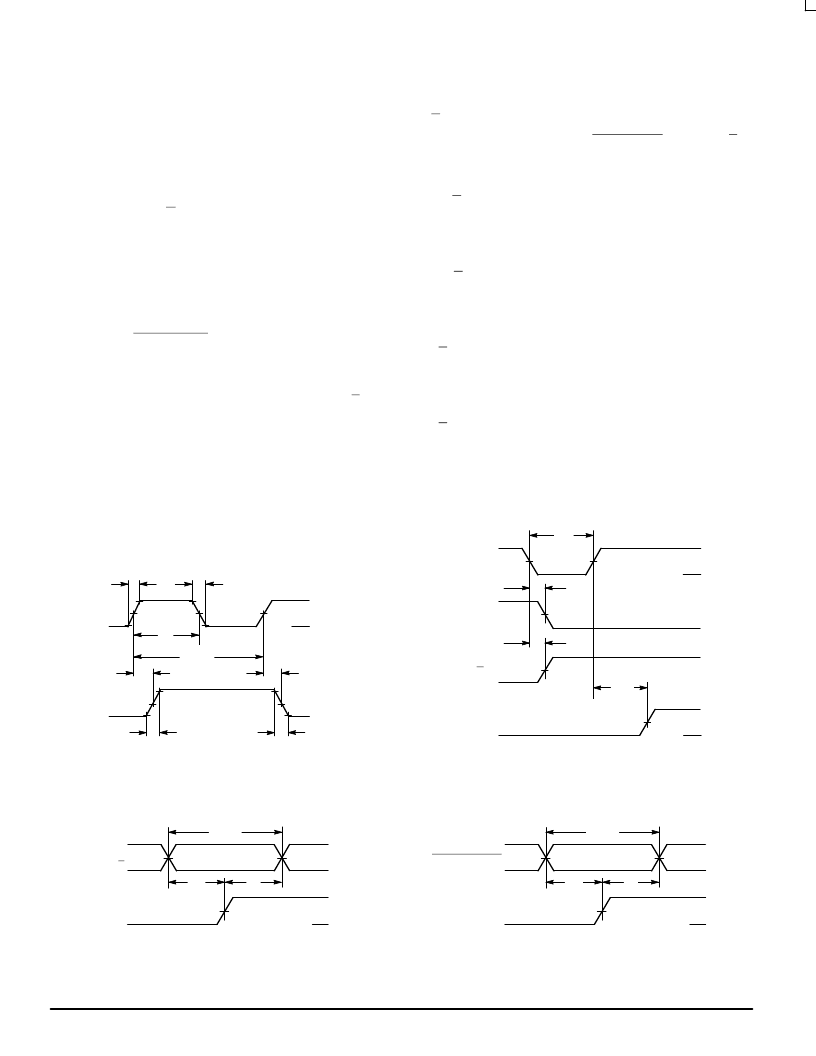
SWITCHING WAVEFORMS
Figure 1.
CLOCK
Q
tr
tf
VCC
GND
90%
50%
10%
90%
50%
10%
tPLH
tPHL
tTLH
tTHL
50%
INPUT
A, B, C,
D, J, OR K
CLOCK
VCC
Figure 2.
VALID
GND
Figure 3.
tw
1/fmax
VCC
GND
tsu
th
50%
Figure 4.
GND
GND
RESET
Q
Q
CLOCK
tPLH
tPHL
trec
tw
VCC
VCC
50%
50%
50%
50%
50%
SERIAL SHIFT
PARALLEL LOAD
CLOCK
VCC
VALID
GND
VCC
GND
tsu
th
50%
相關(guān)PDF資料 |
PDF描述 |
|---|---|
| MC74HC20AD | Dual 4-Input NAND Gate |
| MC74HC20 | Dual 4-Input NAND Gate |
| MC74HC20A | Dual 4-Input NAND Gate |
| MC74HC20ADT | Dual 4-Input NAND Gate |
| MC74HC20AN | Dual 4-Input NAND Gate |
相關(guān)代理商/技術(shù)參數(shù) |
參數(shù)描述 |
|---|---|
| MC74HC1G00DFT1 | 功能描述:邏輯門(mén) 2-6V Single 2-Input RoHS:否 制造商:Texas Instruments 產(chǎn)品:OR 邏輯系列:LVC 柵極數(shù)量:2 線(xiàn)路數(shù)量(輸入/輸出):2 / 1 高電平輸出電流:- 16 mA 低電平輸出電流:16 mA 傳播延遲時(shí)間:3.8 ns 電源電壓-最大:5.5 V 電源電壓-最小:1.65 V 最大工作溫度:+ 125 C 安裝風(fēng)格:SMD/SMT 封裝 / 箱體:DCU-8 封裝:Reel |
| MC74HC1G00DFT1G | 功能描述:邏輯門(mén) 2-6V Single 2-Input NAND RoHS:否 制造商:Texas Instruments 產(chǎn)品:OR 邏輯系列:LVC 柵極數(shù)量:2 線(xiàn)路數(shù)量(輸入/輸出):2 / 1 高電平輸出電流:- 16 mA 低電平輸出電流:16 mA 傳播延遲時(shí)間:3.8 ns 電源電壓-最大:5.5 V 電源電壓-最小:1.65 V 最大工作溫度:+ 125 C 安裝風(fēng)格:SMD/SMT 封裝 / 箱體:DCU-8 封裝:Reel |
| MC74HC1G00DFT1GH | 制造商:Rochester Electronics LLC 功能描述: 制造商:ON Semiconductor 功能描述: |
| MC74HC1G00DFT2 | 功能描述:邏輯門(mén) 2-6V Single 2-Input RoHS:否 制造商:Texas Instruments 產(chǎn)品:OR 邏輯系列:LVC 柵極數(shù)量:2 線(xiàn)路數(shù)量(輸入/輸出):2 / 1 高電平輸出電流:- 16 mA 低電平輸出電流:16 mA 傳播延遲時(shí)間:3.8 ns 電源電壓-最大:5.5 V 電源電壓-最小:1.65 V 最大工作溫度:+ 125 C 安裝風(fēng)格:SMD/SMT 封裝 / 箱體:DCU-8 封裝:Reel |
| MC74HC1G00DFT2G | 功能描述:邏輯門(mén) 2-6V Single 2-Input NAND RoHS:否 制造商:Texas Instruments 產(chǎn)品:OR 邏輯系列:LVC 柵極數(shù)量:2 線(xiàn)路數(shù)量(輸入/輸出):2 / 1 高電平輸出電流:- 16 mA 低電平輸出電流:16 mA 傳播延遲時(shí)間:3.8 ns 電源電壓-最大:5.5 V 電源電壓-最小:1.65 V 最大工作溫度:+ 125 C 安裝風(fēng)格:SMD/SMT 封裝 / 箱體:DCU-8 封裝:Reel |
發(fā)布緊急采購(gòu),3分鐘左右您將得到回復(fù)。