- 您現在的位置:買賣IC網 > PDF目錄371043 > MC68331CPV16 (MOTOROLA INC) User’s Manual PDF資料下載
參數資料
| 型號: | MC68331CPV16 |
| 廠商: | MOTOROLA INC |
| 元件分類: | 微控制器/微處理器 |
| 英文描述: | User’s Manual |
| 中文描述: | 32-BIT, 16.78 MHz, MICROCONTROLLER, PQFP144 |
| 封裝: | TQFP-144 |
| 文件頁數: | 170/254頁 |
| 文件大小: | 1354K |
| 代理商: | MC68331CPV16 |
第1頁第2頁第3頁第4頁第5頁第6頁第7頁第8頁第9頁第10頁第11頁第12頁第13頁第14頁第15頁第16頁第17頁第18頁第19頁第20頁第21頁第22頁第23頁第24頁第25頁第26頁第27頁第28頁第29頁第30頁第31頁第32頁第33頁第34頁第35頁第36頁第37頁第38頁第39頁第40頁第41頁第42頁第43頁第44頁第45頁第46頁第47頁第48頁第49頁第50頁第51頁第52頁第53頁第54頁第55頁第56頁第57頁第58頁第59頁第60頁第61頁第62頁第63頁第64頁第65頁第66頁第67頁第68頁第69頁第70頁第71頁第72頁第73頁第74頁第75頁第76頁第77頁第78頁第79頁第80頁第81頁第82頁第83頁第84頁第85頁第86頁第87頁第88頁第89頁第90頁第91頁第92頁第93頁第94頁第95頁第96頁第97頁第98頁第99頁第100頁第101頁第102頁第103頁第104頁第105頁第106頁第107頁第108頁第109頁第110頁第111頁第112頁第113頁第114頁第115頁第116頁第117頁第118頁第119頁第120頁第121頁第122頁第123頁第124頁第125頁第126頁第127頁第128頁第129頁第130頁第131頁第132頁第133頁第134頁第135頁第136頁第137頁第138頁第139頁第140頁第141頁第142頁第143頁第144頁第145頁第146頁第147頁第148頁第149頁第150頁第151頁第152頁第153頁第154頁第155頁第156頁第157頁第158頁第159頁第160頁第161頁第162頁第163頁第164頁第165頁第166頁第167頁第168頁第169頁當前第170頁第171頁第172頁第173頁第174頁第175頁第176頁第177頁第178頁第179頁第180頁第181頁第182頁第183頁第184頁第185頁第186頁第187頁第188頁第189頁第190頁第191頁第192頁第193頁第194頁第195頁第196頁第197頁第198頁第199頁第200頁第201頁第202頁第203頁第204頁第205頁第206頁第207頁第208頁第209頁第210頁第211頁第212頁第213頁第214頁第215頁第216頁第217頁第218頁第219頁第220頁第221頁第222頁第223頁第224頁第225頁第226頁第227頁第228頁第229頁第230頁第231頁第232頁第233頁第234頁第235頁第236頁第237頁第238頁第239頁第240頁第241頁第242頁第243頁第244頁第245頁第246頁第247頁第248頁第249頁第250頁第251頁第252頁第253頁第254頁
MOTOROLA
7-12
GENERAL-PURPOSE TIMER
MC68331
USER’S MANUAL
7
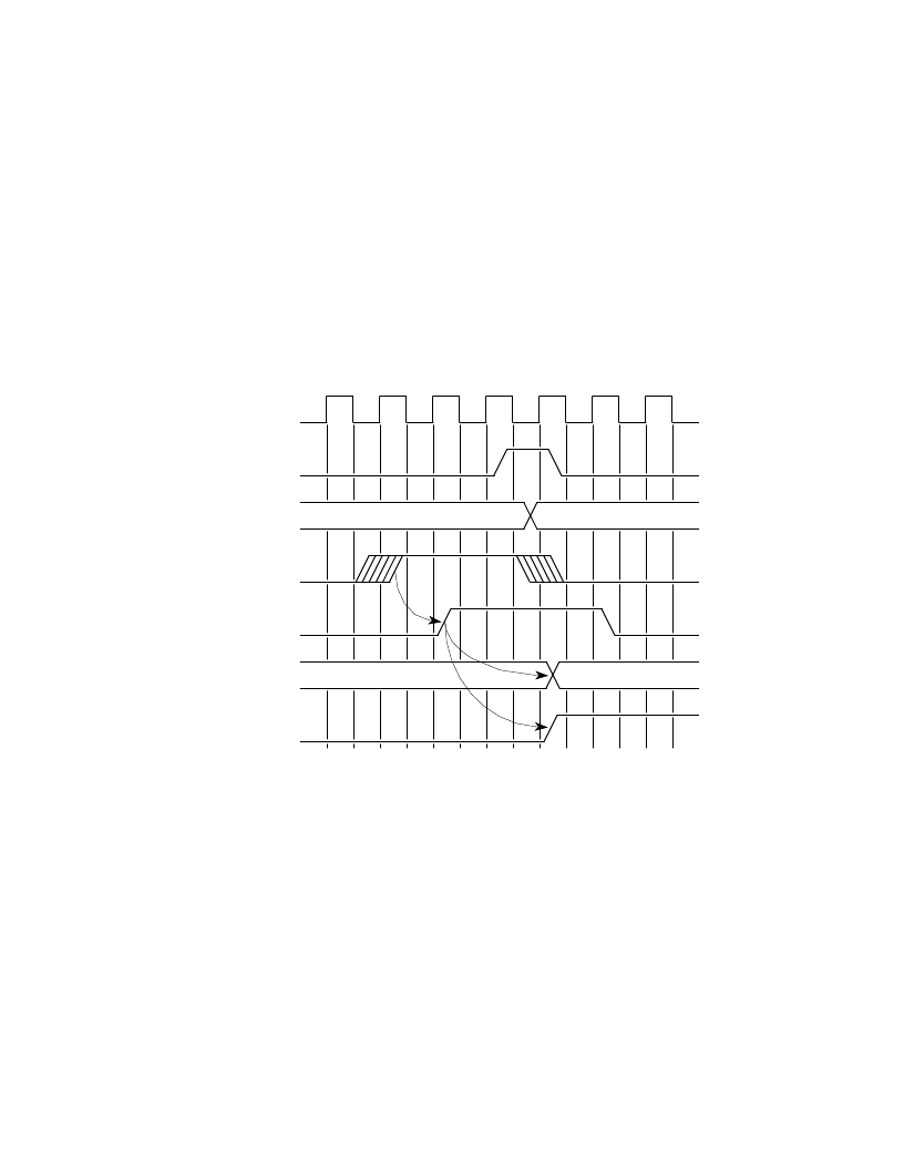
synchronized with the system clock so that latching of TCNT content and counter in-
crementation occur on opposite half-cycles of the system clock. Inputs have hystere-
sis. Capture of any transition longer than two system clocks is guaranteed; any
transition shorter than one system clock has no effect.
Figure 7-4
shows the relationship of system clock to synchronizer output. The value
latched into the capture register is the value of the counter several system clock cycles
after the transition that triggers the edge detection logic. There can be up to one clock
cycle of uncertainty in latching of the input transition. Maximum time is determined by
the system clock frequency.
The input capture register is a 16-bit register. A word access is required to ensure co-
herency. If coherency is not required, byte accesses can be used to read the register.
Input capture registers can be read at any time without affecting their values.
Figure 7-4 Input Capture Timing Example
An input capture occurs every time a selected edge is detected, even when the input
capture status flag is set. This means that the value read from the input capture regis-
ter corresponds to the most recent edge detected, which may not be the edge that
caused the status flag to be set.
7.8.3 Output Compare Functions
Each GPT output compare pin has an associated 16-bit compare register and a 16-bit
comparator. Each output compare function has an associated status flag, and can
cause the GPT to make an interrupt service request. Output compare logic is designed
to prevent false compares during data transition times.
1153A
CAPTURE/COMPARE
CLOCK
CAPTURE REGISTER
$0102
SYNCHRONIZER
OUTPUT
ICF FLAG
EXTERNAL PIN
TCNT
$0102
$0101
F
SYS
(PH1)
相關PDF資料 |
PDF描述 |
|---|---|
| MC68331MFV20 | User’s Manual |
| MC68331MPV16 | User’s Manual |
| MC68331MPV20 | User’s Manual |
| MC68331VFC16 | User’s Manual |
| MC68331VFC20 | User’s Manual |
相關代理商/技術參數 |
參數描述 |
|---|---|
| MC68331CPV16B1 | 制造商:Rochester Electronics LLC 功能描述:32BIT MCU,GPT,SIM,QSM - Bulk |
| MC68331CPV20 | 制造商:Rochester Electronics LLC 功能描述:32BIT MCU,GPT,SIM,QSM - Bulk |
| MC68331CPV20B1 | 制造商:Rochester Electronics LLC 功能描述:32BIT MCU,GPT,SIM,QSM - Bulk |
| MC68331CPV25 | 制造商:Rochester Electronics LLC 功能描述:32BIT MCU,GPT,SIM,QSM - Bulk |
| MC68331LPV20 | 制造商:Motorola Inc 功能描述: |
發(fā)布緊急采購,3分鐘左右您將得到回復。