- 您現(xiàn)在的位置:買賣IC網(wǎng) > PDF目錄382305 > MC33888 (Motorola, Inc.) Quad High-Side and Octal Low-Side Switch for Automotive PDF資料下載
參數(shù)資料
| 型號: | MC33888 |
| 廠商: | Motorola, Inc. |
| 英文描述: | Quad High-Side and Octal Low-Side Switch for Automotive |
| 中文描述: | 四高邊和八路低端汽車開關 |
| 文件頁數(shù): | 23/32頁 |
| 文件大小: | 667K |
| 代理商: | MC33888 |
第1頁第2頁第3頁第4頁第5頁第6頁第7頁第8頁第9頁第10頁第11頁第12頁第13頁第14頁第15頁第16頁第17頁第18頁第19頁第20頁第21頁第22頁當前第23頁第24頁第25頁第26頁第27頁第28頁第29頁第30頁第31頁第32頁
MOTOROLA ANALOG INTEGRATED CIRCUIT DEVICE DATA
33888
23
MODES OF OPERATION
Watchdog and Fail-Safe Operation
The watchdog is enabled and a timeout is started when the
WAKE or
RST
transitions from logic [0] to logic [1]. The WAKE
input is capable of being pulled up to V
PWR
with a series limiting
resistance that limits the internal clamp current. The timeout is
a multiple of an internal oscillator. As long as the WDIN terminal
or the WD bit (D15) of an incoming SPI message is toggled
within the minimum watchdog timeout, WDTO (or a divided
value configured during a WDCSCR message), then the device
will operate normally. If the watchdog timeout occurs before the
WD bit or the WDIN terminal is toggled, then the device will
revert to a Fail-Safe mode until the device is reinitialized (if the
FSI terminal is left disconnected).
During Fail-Safe mode, all outputs will be OFF except for
HS0 and HS2, which will be driven ON regardless of the state
of the various direct inputs and modes (
Table 5
). The device
can be brought out of the Fail-Safe mode by transitioning the
WAKE and
RST
terminals from logic [1] to logic [0]. In the event
the WAKE terminal was not transitioned to a logic [1] during
normal operation and the watchdog times out, then the device
can be brought out of fail-safe by bringing the
RST
to a logic [0].
If the FSI terminal is tied to GND, then the watchdog, and
therefore fail-safe operation, will be disabled.
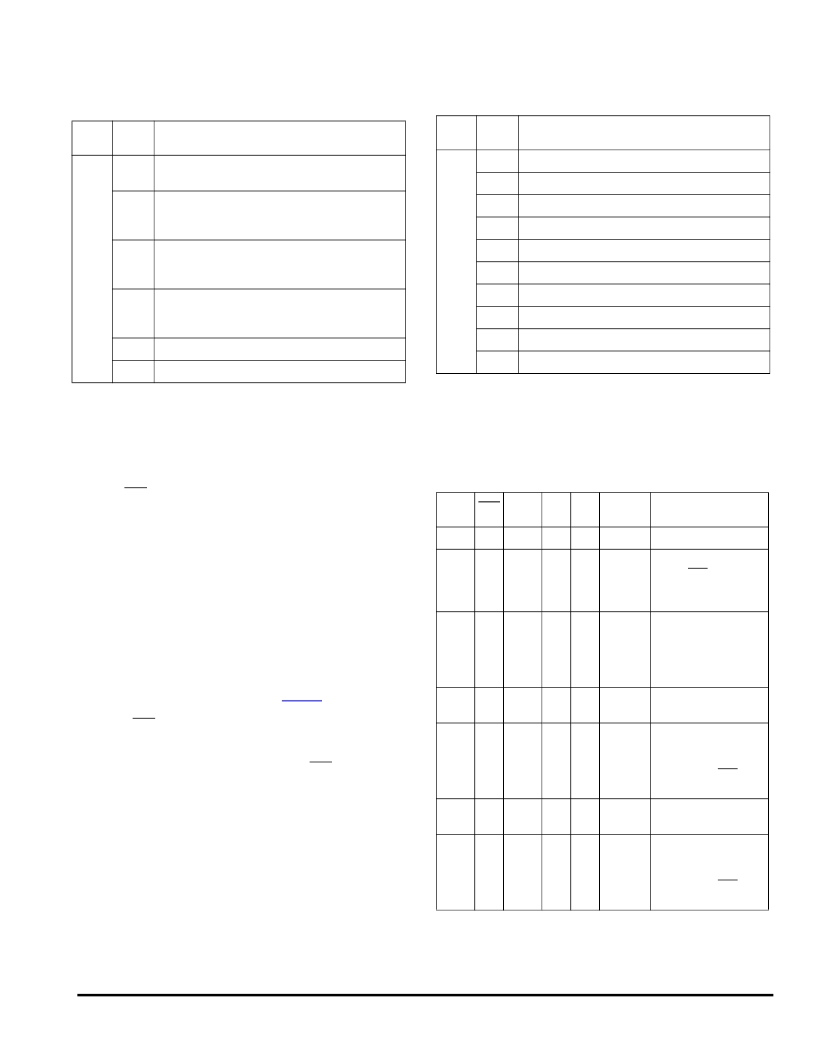
Table 4. Serial Output Bit Assignment
Bit Sig
SO
Msg Bit
Message Bit Description
MSB
OD15
Reflects the state of the Watchdog bit from the
previously clocked-in message.
OD14
If OD15 is logic [0], then this bit will reflect the state
of the direct input IHS0. If OD15 is logic [1], then this
bit will reflect the state of IHS2.
OD13
If OD15 is logic [0], then this bit will reflect the state
of the direct input IHS1. If OD15 is logic [1], then this
bit will reflect the state of IHS3.
OD12
If OD15 is logic [0], then this bit will reflect the state
of the input FSI. If OD15 is logic [1], then this bit will
reflect the state of the input WAKE.
OD11
Reports the absence or presence of a fault on LS11.
OD10
Reports the absence or presence of a fault on LS10.
Bit Sig
SO
Msg Bit
Message Bit Description
OD9
Reports the absence or presence of a fault on LS9.
OD8
Reports the absence or presence of a fault on LS8.
OD7
Reports the absence or presence of a fault on LS7.
OD6
Reports the absence or presence of a fault on LS6.
OD5
Reports the absence or presence of a fault on LS5.
OD4
Reports the absence or presence of a fault on LS4.
OD3
Reports the absence or presence of a fault on HS3.
OD2
Reports the absence or presence of a fault on HS2.
OD1
Reports the absence or presence of a fault on HS1.
LSB
OD0
Reports the absence or presence of a fault on HS0.
Table 4. Serial Output Bit Assignment (continued)
Table 5. Fail-Safe Operation and Transitions
to Other 33888 Modes
WAKE RST WDTO HS0 HS2
LS[4:11],
HS[1,3]
Comments
0
0
x
OFF OFF
OFF
Device in Sleep mode.
1
0
NO
OFF OFF
OFF
All outputs are OFF.
When
RST
transitions
to logic [1], device is in
default.
1
0
YES
ON
ON
OFF
Fail-Safe mode.
Device reset into
Default mode by
transitioning WAKE to
logic [0].
0
1
NO
S
S
S
Device in Normal
operating mode.
0
1
YES
ON
ON
OFF
Fail-Safe mode.
Device reset into
Default mode by
transitioning
RST
to
logic [0].
1
1
NO
S
S
S
Device in Normal
operating mode.
1
1
YES
ON
ON
OFF
Fail-Safe mode.
Device reset into
Default mode by
transitioning
RST
and
WAKE to logic [0].
Assumptions: Normal operating voltage and junction temperatures,
FSI terminal floating.
x=Don’t care.
S=State determined by SPI and/or direct input configurations.
F
Freescale Semiconductor, Inc.
For More Information On This Product,
Go to: www.freescale.com
n
.
相關PDF資料 |
PDF描述 |
|---|---|
| MC33888FB | Quad High-Side and Octal Low-Side Switch for Automotive |
| MC33888FBR2 | Quad High-Side and Octal Low-Side Switch for Automotive |
| MC33972 | Multiple Switch Detection Interface with Suppressed Wake-Up |
| MC33972DWB | Multiple Switch Detection Interface with Suppressed Wake-Up |
| MC33972EW | Multiple Switch Detection Interface with Suppressed Wake-Up |
相關代理商/技術參數(shù) |
參數(shù)描述 |
|---|---|
| MC33888APNBR2 | 制造商:Freescale Semiconductor 功能描述: 制造商:FREESCALE-SEMI 功能描述: |
| MC33888FB | 功能描述:電源開關 IC - 配電 QHSOLSS RoHS:否 制造商:Exar 輸出端數(shù)量:1 開啟電阻(最大值):85 mOhms 開啟時間(最大值):400 us 關閉時間(最大值):20 us 工作電源電壓:3.2 V to 6.5 V 電源電流(最大值): 最大工作溫度:+ 85 C 安裝風格:SMD/SMT 封裝 / 箱體:SOT-23-5 |
| MC33888FBR2 | 功能描述:電源開關 IC - 配電 QHSOLSS RoHS:否 制造商:Exar 輸出端數(shù)量:1 開啟電阻(最大值):85 mOhms 開啟時間(最大值):400 us 關閉時間(最大值):20 us 工作電源電壓:3.2 V to 6.5 V 電源電流(最大值): 最大工作溫度:+ 85 C 安裝風格:SMD/SMT 封裝 / 箱體:SOT-23-5 |
| MC33888PNB | 制造商:FREESCALE-SEMI 功能描述: |
| MC33888PNBR2 | 制造商:FREESCALE-SEMI 功能描述: |
發(fā)布緊急采購,3分鐘左右您將得到回復。