- 您現(xiàn)在的位置:買賣IC網(wǎng) > PDF目錄385565 > MC14572UB (ON SEMICONDUCTOR) Hex Gate(六角門) PDF資料下載
參數(shù)資料
| 型號: | MC14572UB |
| 廠商: | ON SEMICONDUCTOR |
| 英文描述: | Hex Gate(六角門) |
| 中文描述: | 六角門(六角門) |
| 文件頁數(shù): | 1/6頁 |
| 文件大小: | 94K |
| 代理商: | MC14572UB |
Semiconductor Components Industries, LLC, 2006
June, 2006 Rev. 6
1
Publication Order Number:
MC14572UB/D
MC14572UB
Hex Gate
The MC14572UB hex functional gate is constructed with MOS
Pchannel and Nchannel enhancement mode devices in a single
monolithic structure. These complementary MOS logic gates find
primary use where low power dissipation and/or high noise immunity
is desired. The chip contains four inverters, one NOR gate and one
NAND gate.
Features
Diode Protection on All Inputs
Single Supply Operation
Supply Voltage Range = 3.0 Vdc to 18 Vdc
NOR Input Pin Adjacent to V
SS
Pin to Simplify Use As An Inverter
NAND Input Pin Adjacent to V
DD
Pin to Simplify Use As An
Inverter
NOR Output Pin Adjacent to Inverter Input Pin For OR Application
NAND Output Pin Adjacent to Inverter Input Pin For AND
Application
Capable of Driving Two LowPower TTL Loads or One LowPower
Schottky TTL Load over the Rated Temperature Range
PbFree Packages are Available*
MAXIMUM RATINGS
(Voltages Referenced to V
SS
)
Parameter
Symbol
Value
Unit
DC Supply Voltage Range
V
DD
0.5 to +18.0
V
Input or Output Voltage Range
(DC or Transient)
V
in
, V
out
0.5 to V
DD
+ 0.5
V
Input or Output Current (DC or Transient)
per Pin
I
in
, I
out
±
10
mA
Power Dissipation, per Package (Note 1)
P
D
500
mW
Ambient Temperature Range
T
A
55 to +125
°
C
Storage Temperature Range
T
stg
65 to +150
°
C
Lead Temperature (8Second Soldering)
T
L
260
°
C
Stresses exceeding Maximum Ratings may damage the device. Maximum
Ratings are stress ratings only. Functional operation above the Recommended
Operating Conditions is not implied. Extended exposure to stresses above the
Recommended Operating Conditions may affect device reliability.
1. Temperature Derating: Plastic “P and D/DW”
Packages: – 7.0 mW/ C From 65 C To 125 C
This device contains protection circuitry to guard against damage due to high
static voltages or electric fields. However, precautions must be taken to avoid
applications of any voltage higher than maximum rated voltages to this
highimpedance circuit. For proper operation, V
in
and V
out
should be constrained
to the range V
SS
(V
in
or V
out
)
V
DD
.
Unused inputs must always be tied to an appropriate logic voltage level
(e.g., either V
SS
or V
DD
). Unused outputs must be left open.
*For additional information on our PbFree strategy and soldering details, please
download the ON Semiconductor Soldering and Mounting Techniques
Reference Manual, SOLDERRM/D.
Device
Package
Shipping
ORDERING INFORMATION
MC14572UBCP
PDIP16
25 Units / Rail
MC14572UBD
SOIC16
48 Units / Rail
MC14572UBDR2
SOIC16
2500/Tape & Reel
MC14572UBF
SOEIAJ16
http://onsemi.com
For information on tape and reel specifications,
including part orientation and tape sizes, please
refer to our Tape and Reel Packaging Specifications
Brochure, BRD8011/D.
50 Units / Rail
MC14572UBDR2G
SOIC16
(PbFree)
2500/Tape & Reel
MC14572UBDG
SOIC16
(PbFree)
48 Units / Rail
MC14572UBCPG
PDIP16
(PbFree)
25 Units / Rail
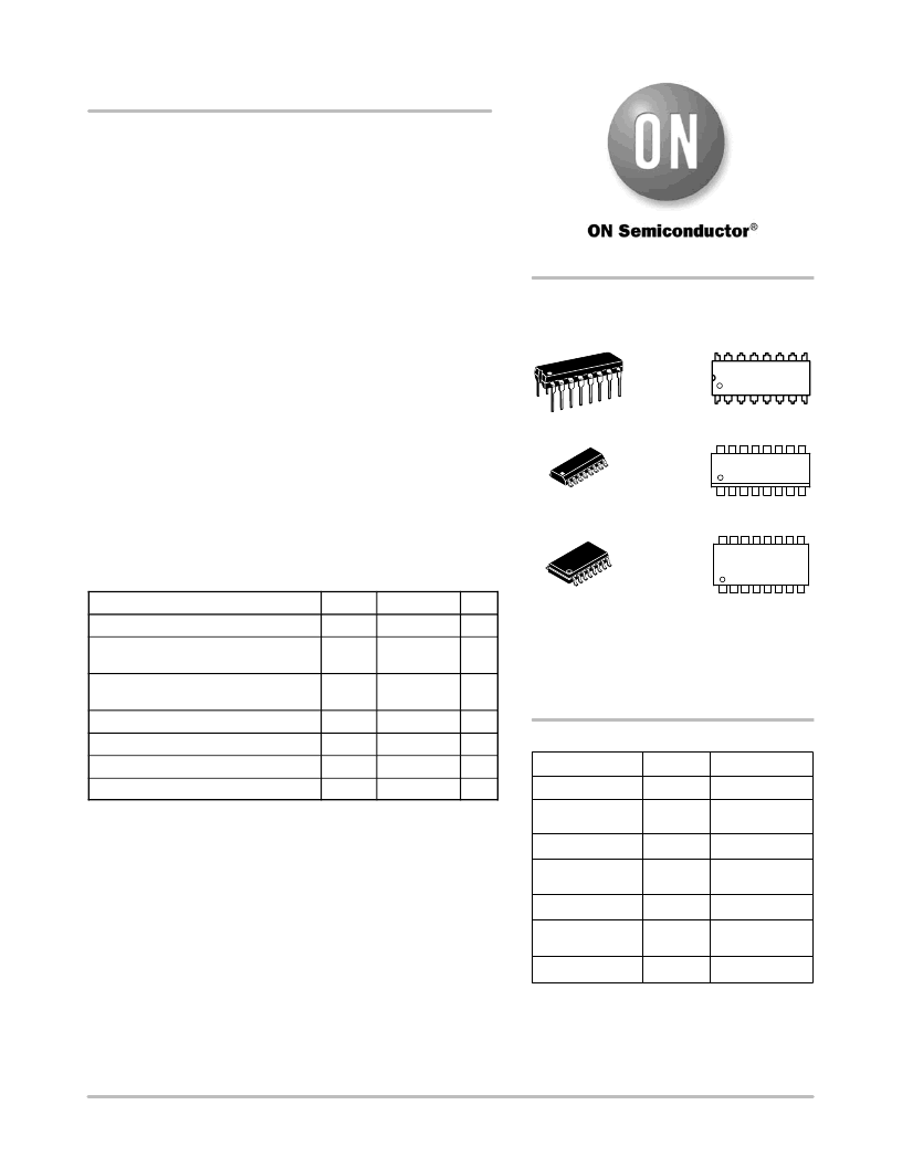
A
WL, L
YY, Y
WW, W = Work Week
G
= PbFree Package
= Assembly Location
= Wafer Lot
= Year
MARKING
DIAGRAMS
PDIP16
P SUFFIX
CASE 648
SOIC16
D SUFFIX
CASE 751B
1
16
14572UBG
AWLYWW
SOEIAJ16
F SUFFIX
CASE 966
1
16
MC14572UB
ALYWG
16
1
MC14572UBCP
AWLYYWWG
1
1
1
相關(guān)PDF資料 |
PDF描述 |
|---|---|
| MC14585BCP | 4-Bit Magnitude Comparator |
| MC14585BD | 4-Bit Magnitude Comparator |
| MC14585BDR2 | 4-Bit Magnitude Comparator |
| MC14585BF | 4-Bit Magnitude Comparator |
| MC14585B | 4 Bit Magnitude Comparator(4位比較器(可級聯(lián))) |
相關(guān)代理商/技術(shù)參數(shù) |
參數(shù)描述 |
|---|---|
| MC14572UBCP | 功能描述:邏輯門 3-18V CMOS Hex RoHS:否 制造商:Texas Instruments 產(chǎn)品:OR 邏輯系列:LVC 柵極數(shù)量:2 線路數(shù)量(輸入/輸出):2 / 1 高電平輸出電流:- 16 mA 低電平輸出電流:16 mA 傳播延遲時間:3.8 ns 電源電壓-最大:5.5 V 電源電壓-最小:1.65 V 最大工作溫度:+ 125 C 安裝風格:SMD/SMT 封裝 / 箱體:DCU-8 封裝:Reel |
| MC14572UBCPG | 功能描述:邏輯門 3-18V CMOS Hex Gate RoHS:否 制造商:Texas Instruments 產(chǎn)品:OR 邏輯系列:LVC 柵極數(shù)量:2 線路數(shù)量(輸入/輸出):2 / 1 高電平輸出電流:- 16 mA 低電平輸出電流:16 mA 傳播延遲時間:3.8 ns 電源電壓-最大:5.5 V 電源電壓-最小:1.65 V 最大工作溫度:+ 125 C 安裝風格:SMD/SMT 封裝 / 箱體:DCU-8 封裝:Reel |
| MC14572UBD | 功能描述:邏輯門 3-18V CMOS Hex RoHS:否 制造商:Texas Instruments 產(chǎn)品:OR 邏輯系列:LVC 柵極數(shù)量:2 線路數(shù)量(輸入/輸出):2 / 1 高電平輸出電流:- 16 mA 低電平輸出電流:16 mA 傳播延遲時間:3.8 ns 電源電壓-最大:5.5 V 電源電壓-最小:1.65 V 最大工作溫度:+ 125 C 安裝風格:SMD/SMT 封裝 / 箱體:DCU-8 封裝:Reel |
| MC14572UBDG | 功能描述:邏輯門 3-18V CMOS Hex Gate RoHS:否 制造商:Texas Instruments 產(chǎn)品:OR 邏輯系列:LVC 柵極數(shù)量:2 線路數(shù)量(輸入/輸出):2 / 1 高電平輸出電流:- 16 mA 低電平輸出電流:16 mA 傳播延遲時間:3.8 ns 電源電壓-最大:5.5 V 電源電壓-最小:1.65 V 最大工作溫度:+ 125 C 安裝風格:SMD/SMT 封裝 / 箱體:DCU-8 封裝:Reel |
| MC14572UBDR2 | 功能描述:邏輯門 3-18V CMOS Hex RoHS:否 制造商:Texas Instruments 產(chǎn)品:OR 邏輯系列:LVC 柵極數(shù)量:2 線路數(shù)量(輸入/輸出):2 / 1 高電平輸出電流:- 16 mA 低電平輸出電流:16 mA 傳播延遲時間:3.8 ns 電源電壓-最大:5.5 V 電源電壓-最小:1.65 V 最大工作溫度:+ 125 C 安裝風格:SMD/SMT 封裝 / 箱體:DCU-8 封裝:Reel |
發(fā)布緊急采購,3分鐘左右您將得到回復。