- 您現(xiàn)在的位置:買賣IC網(wǎng) > PDF目錄385565 > MC14585B (ON SEMICONDUCTOR) 4 Bit Magnitude Comparator(4位比較器(可級(jí)聯(lián))) PDF資料下載
參數(shù)資料
| 型號(hào): | MC14585B |
| 廠商: | ON SEMICONDUCTOR |
| 英文描述: | 4 Bit Magnitude Comparator(4位比較器(可級(jí)聯(lián))) |
| 中文描述: | 4位數(shù)值比較(4位比較器(可級(jí)聯(lián))) |
| 文件頁數(shù): | 1/7頁 |
| 文件大小: | 103K |
| 代理商: | MC14585B |
Semiconductor Components Industries, LLC, 2006
June, 2006 Rev. 6
1
Publication Order Number:
MC14585B/D
MC14585B
4Bit Magnitude Comparator
The MC14585B 4Bit Magnitude Comparator is constructed with
complementary MOS (CMOS) enhancement mode devices. The circuit
has eight comparing inputs (A3, B3, A2, B2, A1, B1, A0, B0), three
cascading inputs (A < B, A = B, and A > B), and three outputs (A < B,
A = B, and A > B). This device compares two 4bit words (A and B)
and determines whether they are “l(fā)ess than”, “equal to”, or “greater
than” by a high level on the appropriate output. For words greater than
4bits, units can be cascaded by connecting outputs (A > B), (A < B),
and (A = B) to the corresponding inputs of the next significant
comparator. Inputs (A < B), (A = B), and (A > B) on the least significant
(first) comparator are connected to a low, a high, and a low, respectively.
Applications include logic in CPU’s, correction and/or detection of
instrumentation conditions, comparator in testers, converters, and
controls.
Features
Diode Protection on All Inputs
Expandable
Applicable to Binary or 8421BCD Code
Supply Voltage Range = 3.0 Vdc to 18 Vdc
Capable of Driving Two LowPower TTL Loads or One LowPower
Schottky TTL Load over the Rated Temperature Range
Can be Cascaded See Figure 3
PbFree Packages are Available*
MAXIMUM RATINGS
(Voltages Referenced to V
SS
)
Parameter
Symbol
Value
Unit
DC Supply Voltage Range
V
DD
V
in
, V
out
0.5 to +18.0
V
Input or Output Voltage Range
(DC or Transient)
0.5 to V
DD
+ 0.5
V
Input or Output Current (DC or Transient)
per Pin
I
in
, I
out
±
10
mA
Power Dissipation per Package (Note 1)
P
D
T
A
T
stg
500
mW
Ambient Temperature Range
55 to +125
°
C
Storage Temperature Range
65 to +150
°
C
Lead Temperature (8Second Soldering)
Stresses exceeding Maximum Ratings may damage the device. Maximum
Ratings are stress ratings only. Functional operation above the Recommended
Operating Conditions is not implied. Extended exposure to stresses above the
Recommended Operating Conditions may affect device reliability.
1. Temperature Derating: Plastic “P and D/DW”
Packages: – 7.0 mW/ C From 65 C To 125 C
This device contains protection circuitry to guard against damage due to high
static voltages or electric fields. However, precautions must be taken to avoid
applications of any voltage higher than maximum rated voltages to this
highimpedance circuit. For proper operation, V
in
and V
out
should be constrained
to the range V
SS
(V
in
or V
out
)
V
DD
.
Unused inputs must always be tied to an appropriate logic voltage level
(e.g., either V
SS
or V
DD
). Unused outputs must be left open.
T
L
260
°
C
*For additional information on our PbFree strategy and soldering details, please
download the ON Semiconductor Soldering and Mounting Techniques
Reference Manual, SOLDERRM/D.
Device
Package
Shipping
ORDERING INFORMATION
MC14585BCP
PDIP16
25 Units / Rail
MC14585BD
SOIC16
48 Units / Rail
MC14585BDR2
SOIC16
2500/Tape & Reel
MC14585BFEL
SOEIAJ16
http://onsemi.com
2000/Tape & Reel
MC14585BFELG
SOEIAJ16
(PbFree)
2000/Tape & Reel
MC14585BDR2G
SOIC16
(PbFree)
2500/Tape & Reel
MC14585BDG
SOIC16
(PbFree)
48 Units / Rail
MC14585BCPG
PDIP16
(PbFree)
25 Units / Rail
For information on tape and reel specifications,
including part orientation and tape sizes, please
refer to our Tape and Reel Packaging Specifications
Brochure, BRD8011/D.
A
WL, L
YY, Y
WW, W = Work Week
G
= PbFree Package
= Assembly Location
= Wafer Lot
= Year
MARKING
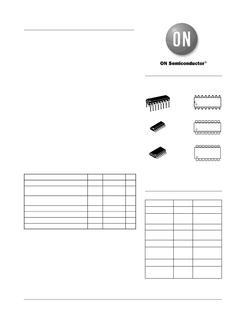
DIAGRAMS
PDIP16
P SUFFIX
CASE 648
SOIC16
D SUFFIX
CASE 751B
1
16
14585BG
AWLYWW
SOEIAJ16
F SUFFIX
CASE 966
1
16
MC14585B
ALYWG
16
1
MC14585BCP
AWLYYWWG
1
1
1
相關(guān)PDF資料 |
PDF描述 |
|---|---|
| MC14598B | 8 Bit Bus Compatible Latches(八位總線型鎖存器) |
| MC1471 | Internally Compensated, High Performance Operational Amplifier |
| MC1489A | Quad Line EIA-232D Receivers(RS-232四線接收器) |
| MC1H3 | High Voltage Power Module Users Guide |
| MC33023DWG | High Speed Single−Ended PWM Controller |
相關(guān)代理商/技術(shù)參數(shù) |
參數(shù)描述 |
|---|---|
| MC14585BALD | 制造商:Motorola Inc 功能描述: |
| MC14585BCL | 制造商:Rochester Electronics LLC 功能描述:- Bulk |
| MC14585BCP | 功能描述:校驗(yàn)器 IC 4-Bit CMOS Magnitude RoHS:否 制造商:STMicroelectronics 產(chǎn)品: 比較器類型: 通道數(shù)量: 輸出類型:Push-Pull 電源電壓-最大:5.5 V 電源電壓-最小:1.1 V 補(bǔ)償電壓(最大值):6 mV 電源電流(最大值):1350 nA 響應(yīng)時(shí)間: 最大工作溫度:+ 125 C 安裝風(fēng)格:SMD/SMT 封裝 / 箱體:SC-70-5 封裝:Reel |
| MC14585BCPG | 功能描述:校驗(yàn)器 IC 4-Bit CMOS Magnitude RoHS:否 制造商:STMicroelectronics 產(chǎn)品: 比較器類型: 通道數(shù)量: 輸出類型:Push-Pull 電源電壓-最大:5.5 V 電源電壓-最小:1.1 V 補(bǔ)償電壓(最大值):6 mV 電源電流(最大值):1350 nA 響應(yīng)時(shí)間: 最大工作溫度:+ 125 C 安裝風(fēng)格:SMD/SMT 封裝 / 箱體:SC-70-5 封裝:Reel |
| MC14585BD | 功能描述:校驗(yàn)器 IC 4-Bit CMOS Magnitude RoHS:否 制造商:STMicroelectronics 產(chǎn)品: 比較器類型: 通道數(shù)量: 輸出類型:Push-Pull 電源電壓-最大:5.5 V 電源電壓-最小:1.1 V 補(bǔ)償電壓(最大值):6 mV 電源電流(最大值):1350 nA 響應(yīng)時(shí)間: 最大工作溫度:+ 125 C 安裝風(fēng)格:SMD/SMT 封裝 / 箱體:SC-70-5 封裝:Reel |
發(fā)布緊急采購(gòu),3分鐘左右您將得到回復(fù)。